


- TLVH431BCDBVTG4 - 集成电路(IC) > 电源管理(PMIC) > 电压基准
- LP3971SQ-O509/NOPB - 集成电路(IC) > 电源管理(PMIC) > 电源管理 - 专用
- THS4513RGTR - 集成电路(IC) > 线性 > 放大器 > 仪器,运算放大器,缓冲器
- SN74LVCH32374AZKER - 集成电路(IC) > 逻辑 > 触发器
- LM4040A30IDCKRE4 - 集成电路(IC) > 电源管理(PMIC) > 电压基准
- THS4001CDR - 集成电路(IC) > 线性 > 放大器 > 仪器,运算放大器,缓冲器
- TPS2346PWR - 集成电路(IC) > 电源管理(PMIC) > 热插拔控制器
- SN74LVT16244BZQLR - 集成电路(IC) > 逻辑 > 缓冲器,驱动器,接收器,收发器
- AM6421BSFGHAALV - 集成电路(IC) > 嵌入式 > 微处理器
- TLK10081CTR - 集成电路(IC) > 接口 > 驱动器,接收器,收发器
- CLC730031/NOPB - 评估板 - 运算放大器
- TPS54821RHLR - 集成电路(IC) > 电源管理(PMIC) > 稳压器 - DC-DC 开关稳压器
- LM2674M-ADJ/NOPB - 集成电路(IC) > 电源管理(PMIC) > 稳压器 - DC-DC 开关稳压器
- TL1431QLPR - 集成电路(IC) > 电源管理(PMIC) > 电压基准
- CD4049UBDT - 集成电路(IC) > 逻辑 > 门和反相器
- MSP430F2616TZQWR - 集成电路(IC) > 嵌入式 > 微控制器
- PCM1702U-JE6 - 集成电路(IC) > 数据采集 > ADC/DAC - 特殊用途
- TM4C1294NCPDTI3 - 集成电路(IC) > 嵌入式 > 微控制器
- CDCLVD1216RGZR - 集成电路(IC) > 时钟/定时 > 时钟缓冲器,驱动器
- TIOS1013DMWR - 集成电路(IC) > 接口 > 驱动器,接收器,收发器


AM3358 - Sitara ARM Cortex-A8 微处理器
AM3358是TI德州仪器公司的一款ARMCortex-A8产品,AM3358是Sitara ARM Cortex-A8 微处理器,本站介绍了AM3358的封装应用图解、特点和优点、功能等,并给出了与AM3358相关的TI元器件型号供参考。
AM3358 - Sitara ARM Cortex-A8 微处理器 - ARMCortex-A8 - Sitara处理器 - 德州仪器
- Up to 1-GHz Sitara™ ARM® Cortex®-A8 32?Bit RISC Processor
- NEON™ SIMD Coprocessor
- 32KB of L1 Instruction and 32KB of Data Cache With Single-Error Detection (Parity)
- 256KB of L2 Cache With Error Correcting Code (ECC)
- 176KB of On-Chip Boot ROM
- 64KB of Dedicated RAM
- Emulation and Debug - JTAG
- Interrupt Controller (up to 128 Interrupt Requests)
- On-Chip Memory (Shared L3 RAM)
- 64KB of General-Purpose On-Chip Memory Controller (OCMC) RAM
- Accessible to All Masters
- Supports Retention for Fast Wakeup
- External Memory Interfaces (EMIF)
- mDDR(LPDDR), DDR2, DDR3, DDR3L Controller:
- mDDR: 200-MHz Clock (400-MHz Data Rate)
- DDR2: 266-MHz Clock (532-MHz Data Rate)
- DDR3: 400-MHz Clock (800-MHz Data Rate)
- DDR3L: 400-MHz Clock (800-MHz Data Rate)
- 16-Bit Data Bus
- 1GB of Total Addressable Space
- Supports One x16 or Two x8 Memory Device Configurations
- General-Purpose Memory Controller (GPMC)
- Flexible 8-Bit and 16-Bit Asynchronous Memory Interface With up to Seven Chip Selects (NAND, NOR, Muxed-NOR, SRAM)
- Uses BCH Code to Support 4-, 8-, or 16-Bit ECC
- Uses Hamming Code to Support 1-Bit ECC
- Error Locator Module (ELM)
- Used in Conjunction With the GPMC to Locate Addresses of Data Errors from Syndrome Polynomials Generated Using a BCH Algorithm
- Supports 4-, 8-, and 16-Bit per 512-Byte Block Error Location Based on BCH Algorithms
- mDDR(LPDDR), DDR2, DDR3, DDR3L Controller:
- Programmable Real-Time Unit Subsystem and Industrial Communication Subsystem (PRU-ICSS)
- Supports Protocols such as EtherCAT®, PROFIBUS, PROFINET, EtherNet/IP™, and More
- Two Programmable Real-Time Units (PRUs)
- 32-Bit Load/Store RISC Processor Capable of Running at 200 MHz
- 8KB of Instruction RAM With Single-Error Detection (Parity)
- 8KB of Data RAM With Single-Error Detection (Parity)
- Single-Cycle 32-Bit Multiplier With 64-Bit Accumulator
- Enhanced GPIO Module Provides Shift-In/Out Support and Parallel Latch on External Signal
- 12KB of Shared RAM With Single-Error Detection (Parity)
- Three 120-Byte Register Banks Accessible by Each PRU
- Interrupt Controller (INTC) for Handling System Input Events
- Local Interconnect Bus for Connecting Internal and External Masters to the Resources Inside the PRU-ICSS
- Peripherals Inside the PRU-ICSS:
- One UART Port With Flow Control Pins, Supports up to 12 Mbps
- One Enhanced Capture (eCAP) Module
- Two MII Ethernet Ports that Support Industrial Ethernet, such as EtherCAT
- One MDIO Port
- Power, Reset, and Clock Management (PRCM) Module
- Controls the Entry and Exit of Stand-By and Deep-Sleep Modes
- Responsible for Sleep Sequencing, Power Domain Switch-Off Sequencing, Wake-Up Sequencing, and Power Domain Switch-On Sequencing
- Clocks
- Integrated 15- to 35-MHz High-Frequency Oscillator Used to Generate a Reference Clock for Various System and Peripheral Clocks
- Supports Individual Clock Enable and Disable Control for Subsystems and Peripherals to Facilitate Reduced Power Consumption
- Five ADPLLs to Generate System Clocks (MPU Subsystem, DDR Interface, USB and Peripherals [MMC and SD, UART, SPI, I2C], L3, L4, Ethernet, GFX [SGX530], LCD Pixel Clock)
- Power
- Two Nonswitchable Power Domains (Real-Time Clock [RTC], Wake-Up Logic [WAKEUP])
- Three Switchable Power Domains (MPU Subsystem [MPU], SGX530 [GFX], Peripherals and Infrastructure [PER])
- Implements SmartReflex™ Class 2B for Core Voltage Scaling Based On Die Temperature, Process Variation, and Performance (Adaptive Voltage Scaling [AVS])
- Dynamic Voltage Frequency Scaling (DVFS)
- Real-Time Clock (RTC)
- Real-Time Date (Day-Month-Year-Day of Week) and Time (Hours-Minutes-Seconds) Information
- Internal 32.768-kHz Oscillator, RTC Logic and 1.1-V Internal LDO
- Independent Power-on-Reset (RTC_PWRONRSTn) Input
- Dedicated Input Pin (EXT_WAKEUP) for External Wake Events
- Programmable Alarm Can be Used to Generate Internal Interrupts to the PRCM (for Wakeup) or Cortex-A8 (for Event Notification)
- Programmable Alarm Can be Used With External Output (PMIC_POWER_EN) to Enable the Power Management IC to Restore Non-RTC Power Domains
- Peripherals
- Up to Two USB 2.0 High-Speed OTG Ports With Integrated PHY
- Up to Two Industrial Gigabit Ethernet MACs (10, 100, 1000 Mbps)
- Integrated Switch
- Each MAC Supports MII, RMII, RGMII, and MDIO Interfaces
- Ethernet MACs and Switch Can Operate Independent of Other Functions
- IEEE 1588v2 Precision Time Protocol (PTP)
- Up to Two Controller-Area Network (CAN) Ports
- Supports CAN Version 2 Parts A and B
- Up to Two Multichannel Audio Serial Ports (McASPs)
- Transmit and Receive Clocks up to 50 MHz
- Up to Four Serial Data Pins per McASP Port With Independent TX and RX Clocks
- Supports Time Division Multiplexing (TDM), Inter-IC Sound (I2S), and Similar Formats
- Supports Digital Audio Interface Transmission (SPDIF, IEC60958-1, and AES-3 Formats)
- FIFO Buffers for Transmit and Receive (256 Bytes)
- Up to Six UARTs
- All UARTs Support IrDA and CIR Modes
- All UARTs Support RTS and CTS Flow Control
- UART1 Supports Full Modem Control
- Up to Two Master and Slave McSPI Serial Interfaces
- Up to Two Chip Selects
- Up to 48 MHz
- Up to Three MMC, SD, SDIO Ports
- 1-, 4- and 8-Bit MMC, SD, SDIO Modes
- MMCSD0 has Dedicated Power Rail for 1.8?V or 3.3-V Operation
- Up to 48-MHz Data Transfer Rate
- Supports Card Detect and Write Protect
- Complies With MMC4.3, SD, SDIO 2.0 Specifications
- Up to Three I2C Master and Slave Interfaces
- Standard Mode (up to 100kHz)
- Fast Mode (up to 400 kHz)
- Up to Four Banks of General-Purpose I/O (GPIO) Pins
- 32 GPIO Pins per Bank (Multiplexed With Other Functional Pins)
- GPIO Pins Can be Used as Interrupt Inputs (up to Two Interrupt Inputs per Bank)
- Up to Three External DMA Event Inputs that can Also be Used as Interrupt Inputs
- Eight 32-Bit General-Purpose Timers
- DMTIMER1 is a 1-ms Timer Used for Operating System (OS) Ticks
- DMTIMER4–DMTIMER7 are Pinned Out
- One Watchdog Timer
- SGX530 3D Graphics Engine
- Tile-Based Architecture Delivering up to 20 Million Polygons per Second
- Universal Scalable Shader Engine (USSE) is a Multithreaded Engine Incorporating Pixel and Vertex Shader Functionality
- Advanced Shader Feature Set in Excess of Microsoft VS3.0, PS3.0, and OGL2.0
- Industry Standard API Support of Direct3D Mobile, OGL-ES 1.1 and 2.0, OpenVG 1.0, and OpenMax
- Fine-Grained Task Switching, Load Balancing, and Power Management
- Advanced Geometry DMA-Driven Operation for Minimum CPU Interaction
- Programmable High-Quality Image Anti-Aliasing
- Fully Virtualized Memory Addressing for OS Operation in a Unified Memory Architecture
- LCD Controller
- Up to 24-Bit Data Output; 8 Bits per Pixel (RGB)
- Resolution up to 2048 × 2048 (With Maximum 126-MHz Pixel Clock)
- Integrated LCD Interface Display Driver (LIDD) Controller
- Integrated Raster Controller
- Integrated DMA Engine to Pull Data from the External Frame Buffer Without Burdening the Processor via Interrupts or a Firmware Timer
- 512-Word Deep Internal FIFO
- Supported Display Types:
- Character Displays - Uses LIDD Controller to Program these Displays
- Passive Matrix LCD Displays - Uses LCD Raster Display Controller to Provide Timing and Data for Constant Graphics Refresh to a Passive Display
- Active Matrix LCD Displays - Uses External Frame Buffer Space and the Internal DMA Engine to Drive Streaming Data to the Panel
- 12-Bit Successive Approximation Register (SAR) ADC
- 200K Samples per Second
- Input can be Selected from any of the Eight Analog Inputs Multiplexed Through an 8:1 Analog Switch
- Can be Configured to Operate as a 4-Wire, 5-Wire, or 8-Wire Resistive Touch Screen Controller (TSC) Interface
- Up to Three 32-Bit eCAP Modules
- Configurable as Three Capture Inputs or Three Auxiliary PWM Outputs
- Up to Three Enhanced High-Resolution PWM Modules (eHRPWMs)
- Dedicated 16-Bit Time-Base Counter With Time and Frequency Controls
- Configurable as Six Single-Ended, Six Dual-Edge Symmetric, or Three Dual-Edge Asymmetric Outputs
- Up to Three 32-Bit Enhanced Quadrature Encoder Pulse (eQEP) Modules
- Device Identification
- Contains Electrical Fuse Farm (FuseFarm) of Which Some Bits are Factory Programmable
- Production ID
- Device Part Number (Unique JTAG ID)
- Device Revision (Readable by Host ARM)
- Contains Electrical Fuse Farm (FuseFarm) of Which Some Bits are Factory Programmable
- Debug Interface Support
- JTAG and cJTAG for ARM (Cortex-A8 and PRCM), PRU-ICSS Debug
- Supports Device Boundary Scan
- Supports IEEE 1500
- DMA
- On-Chip Enhanced DMA Controller (EDMA) has Three Third-Party Transfer Controllers (TPTCs) and One Third-Party Channel Controller (TPCC), Which Supports up to 64 Programmable Logical Channels and Eight QDMA Channels. EDMA is Used for:
- Transfers to and from On-Chip Memories
- Transfers to and from External Storage (EMIF, GPMC, Slave Peripherals)
- On-Chip Enhanced DMA Controller (EDMA) has Three Third-Party Transfer Controllers (TPTCs) and One Third-Party Channel Controller (TPCC), Which Supports up to 64 Programmable Logical Channels and Eight QDMA Channels. EDMA is Used for:
- Inter-Processor Communication (IPC)
- Integrates Hardware-Based Mailbox for IPC and Spinlock for Process Synchronization Between Cortex-A8, PRCM, and PRU-ICSS
- Mailbox Registers that Generate Interrupts
- Four Initiators (Cortex-A8, PRCM, PRU0, PRU1)
- Spinlock has 128 Software-Assigned Lock Registers
- Mailbox Registers that Generate Interrupts
- Integrates Hardware-Based Mailbox for IPC and Spinlock for Process Synchronization Between Cortex-A8, PRCM, and PRU-ICSS
- Security
- Crypto Hardware Accelerators (AES, SHA, RNG)
- Boot Modes
- Boot Mode is Selected Through Boot Configuration Pins Latched on the Rising Edge of the PWRONRSTn Reset Input Pin
- Packages:
- 298-Pin S-PBGA-N298 Via Channel Package (ZCE Suffix), 0.65-mm Ball Pitch
- 324-Pin S-PBGA-N324 Package (ZCZ Suffix), 0.80-mm Ball Pitch
- Gaming Peripherals
- Home and Industrial Automation
- Consumer Medical Appliances
- Printers
- Smart Toll Systems
- Connected Vending Machines
- Weighing Scales
- Educational Consoles
- Advanced Toys
The AM335x microprocessors, based on the ARM Cortex-A8 processor, are enhanced with image, graphics processing, peripherals and industrial interface options such as EtherCAT and PROFIBUS. The devices support high-level operating systems (HLOS). Linux® and Android™ are available free of charge from TI.
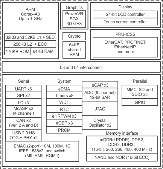
The AM335x microprocessor contain the subsystems shown in Figure 1-1 and a brief description of each follows:
The microprocessor unit (MPU) subsystem is based on the ARM Cortex-A8 processor and the PowerVR SGX™ Graphics Accelerator subsystem provides 3D graphics acceleration to support display and gaming effects.
The PRU-ICSS is separate from the ARM core, allowing independent operation and clocking for greater efficiency and flexibility. The PRU-ICSS enables additional peripheral interfaces and real-time protocols such as EtherCAT, PROFINET, EtherNet/IP, PROFIBUS, Ethernet Powerlink, Sercos, and others. Additionally, the programmable nature of the PRU-ICSS, along with its access to pins, events and all system-on-chip (SoC) resources, provides flexibility in implementing fast, real-time responses, specialized data handling operations, custom peripheral interfaces, and in offloading tasks from the other processor cores of SoC.
| PART NUMBER | PACKAGE | BODY SIZE |
|---|---|---|
| AM3359ZCZ | NFBGA (324) | 15.0 mm × 15.0 mm |
| AM3358ZCZ | NFBGA (324) | 15.0 mm × 15.0 mm |
| AM3357ZCZ | NFBGA (324) | 15.0 mm × 15.0 mm |
| AM3356ZCZ, AM3356ZCE | NFBGA (324), NFBGA (298) | 15.0 mm × 15.0 mm, 13.0 mm × 13.0 mm |
| AM3354ZCZ, AM3354ZCE | NFBGA (324), NFBGA (298) | 15.0 mm × 15.0 mm, 13.0 mm × 13.0 mm |
| AM3352ZCZ, AM3352ZCE | NFBGA (324), NFBGA (298) | 15.0 mm × 15.0 mm, 13.0 mm × 13.0 mm |
| AM3351ZCE | NFBGA (298) | 13.0 mm × 13.0 mm |
- TS5A4596 - 8Ω SPST 5V/3.3V 单通道模拟开关
- SN54LVT8980A - 具有 8 位发生器的嵌入式测试总线控制器 IEEE STD 1149.1 (JTAG) TAP 主控方
- LM2840 - 100 mA up to 42V Input Step-Down DC/DC Regulator in Thin SOT-23
- PTN78060W - 3A、宽输入、可调节开关稳压器模块
- ADS7250 - 双通道、1MSPS、16/14/12 位同步采样模数转换器
- TPS61181A - 用于笔记本电脑应用的 6 串 LED 驱动器
- TPS70845 - 具有 SVS 和独立启用的双路输出 LDO
- RM48L950 - 16/32-Bit RISC Flash Microcontroller
- TS3L500 - 具有低而平坦的导通电阻的 16 位到 8 位 SPDT 千兆 LAN 交换机
- TPS2592ZA - 具有过压保护和阻断 FET 控制功能的 5V/12V 熔丝

