


- TL322IP - 集成电路(IC) > 线性 > 放大器 > 仪器,运算放大器,缓冲器
- 74AVCA164245ZQLR - 集成电路(IC) > 逻辑 > 转换器,电平移位器
- BOOST-TUSS4440 - 开发板,套件,编程器 > 评估板 > 扩展板,子卡
- THS4551IRGTR - 集成电路(IC) > 线性 > 放大器 > 仪器,运算放大器,缓冲器
- MSP430F1222IRHBR - 集成电路(IC) > 嵌入式 > 微控制器
- MC1458P - 集成电路(IC) > 线性 > 放大器 > 仪器,运算放大器,缓冲器
- DS100BR111EVK/NOPB - 开发板,套件,编程器 > 评估板 > 评估和演示板及套件
- LM4549AVH - 集成电路(IC) > 接口 > 编解码器
- TLV2241TDR - 集成电路(IC) > 线性 > 放大器 > 仪器,运算放大器,缓冲器
- CDCVF855PWRG4 - 集成电路(IC) > 时钟/定时 > 时钟发生器,PLL,频率合成器
- PCA9535RTWR - 集成电路(IC) > 接口 > I/O 扩展器
- LM2937ESX-10/NOPB - 集成电路(IC) > 电源管理(PMIC) > 稳压器 - 线性
- TPS62110RSATG4 - 集成电路(IC) > 电源管理(PMIC) > 稳压器 - DC-DC 开关稳压器
- SN74ACT165WBQBRQ1 - 集成电路(IC) > 逻辑 > 移位寄存器
- CD74HC30PWR - 集成电路(IC) > 逻辑 > 门和反相器
- TPA3113D2EVM - 开发板,套件,编程器 > 评估板 > 音频放大器评估板
- UCC35702D - 集成电路(IC) > 电源管理(PMIC) > DC-DC 开关控制器
- ADS7863IDBQR - 集成电路(IC) > 数据采集 > 模数转换器(ADC)
- MSP430F2618TZQW - 集成电路(IC) > 嵌入式 > 微控制器
- PT5402A - 板安装电源 > 直流转换器


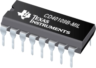
CD40109B-MIL - CMOS 四路低向高电压位转换器(20V 额定电压)
CD40109B-MIL是TI德州仪器公司的一款单向电压转换产品,CD40109B-MIL是CMOS 四路低向高电压位转换器(20V 额定电压),本站介绍了CD40109B-MIL的封装应用图解、特点和优点、功能等,并给出了与CD40109B-MIL相关的TI元器件型号供参考。
CD40109B-MIL - CMOS 四路低向高电压位转换器(20V 额定电压) - 单向电压转换 - 电压电平转换 - 德州仪器
CD40109B contains four low-to-high-voltage level-shifting circuits. Each circuit will shift a low-voltage digital-logic input signal (A, B, C, D) with logical 1 = VCC and logical 0 = VSS to a higher-voltage output signal (E, F, G, H) with logical 1 = VDD and logical 0 = VSS.
The CD40109, unlike other low-to-high level-shifting circuits, does not require the presence of the high-voltage supply (VDD) before the application of either the low-voltage supply (VCC) or the input signals. There are no restrictions on the sequence of application of VDD, VCC, or the input signals. In addition, with one exception there are no restrictions on the relative magnitudes of the supply voltages or input signals within the device maximum ratings, provided that the input signal swings between VSS and at least 0.7 VCC; VCC may exceed VDD, and input signals may exceed VCC and VDD. When operated in the mode VCC > VDD, the CD40109 will operate as a high-to-low level-shifter.
The CD40109 also features individual three-state output capability. A low level on any of the separately enabled three-state output controls produces a high-impedance state in the corresponding output.
The CD40109B-Series types are supplied in 16-lead ceramic dual-in-line packages (F3A suffix), 16-lead dual-in-line plastic packages (E suffix), 16-lead small-outline packages (NSR suffix), and 16-lead thin shrink small-outline packages (PW and PWR suffixes).
- Independence of power supply sequence considerations - VCC can exceed VDD, input signals can exceed both VCC and VDD
- Up and down level-shifting capability
- Three-state outputs with separate enable controls
- Standardized, symmetrical output characteristics
- 100% tested for quiescent current at 20 V
- Maximum input current of 1 uA at 18 V over full package-temperature range; 100 nA at 18 V and 25°C
- Noise margin (full package-temperature range): = 1 V at VCC = 5 V, VDD = 10 V = 2 V at VCC = 10 V, VDD = 15 V
- 5-V, 10-V, and 15-V parametric ratings
- Meets all requirements of JEDEC Tentative Standard No. 13B, "Standard Specifications for Description of 'B' Series CMOS Devices"
- Applications:
- High-or-low level-shifting with three-state outputs for unidirectional or bidirectional bussing.
- Isolation of logic subsystems using separate power supplies from supply sequencing, supply loss and supply regulation considerations
Data sheet acquired from Harris Semiconductor
- ADS1601 - 16 位 1.25MSPS 模数转换器
- TPS54613 - 具有 1.5V 输出的低输入电压 6A 同步降压转换器
- MSP430F1101A - 16 位超低功耗微控制器,具有 1kB 闪存、128B RAM 和比较器
- LM48100Q-Q1 - 具有输出故障检测和音量控制功能的单声道 1.3W 音频功率放大器
- LP8552 - High-Efficiency LED Backlight Driver for Notebooks
- ONET1130EP - ONET1130EP 具有调制器驱动器的 11.7Gbps 收发器
- TPS2069 - 限流配电开关
- LM4125 - 精密微功耗低压降电压基准
- MSP430F6659 - MSP430F563xA 混合信号微控制器
- TMS320VC5402A - 定点数字信号处理器

