



- THS4222D - 集成电路(IC) > 线性 > 放大器 > 仪器,运算放大器,缓冲器
- LM324J - 集成电路(IC) > 线性 > 放大器 > 仪器,运算放大器,缓冲器
- LM4549BVHX/NOPB - 集成电路(IC) > 接口 > 编解码器
- SN74S374NSRE4 - 逻辑 - 触发器
- AMC7812BSRGCT - 集成电路(IC) > 数据采集 > ADC/DAC - 特殊用途
- ADS1203IPWRG4 - 集成电路(IC) > 数据采集 > ADC/DAC - 特殊用途
- LMP7300MME/NOPB - 集成电路(IC) > 线性 > 比较器
- SN74ABT8646DWRE4 - 逻辑 - 专用逻辑
- ADC12081EVAL - 评估板 - 模数转换器(ADC)
- 74ABT16543DGGRG4 - 集成电路(IC) > 逻辑 > 缓冲器,驱动器,接收器,收发器
- DAC7541AKPG4 - 集成电路(IC) > 数据采集 > 数模转换器(DAC)
- SN65HVD31D - 集成电路(IC) > 接口 > 驱动器,接收器,收发器
- LM2991T/NOPB - 集成电路(IC) > 电源管理(PMIC) > 稳压器 - 线性
- TPS7A9001DSKR - 集成电路(IC) > 电源管理(PMIC) > 稳压器 - 线性
- TMDX324B61E-07 - 开发板编程器配件
- SN65HVS880PWPR - 集成电路(IC) > 接口 > 串行器,解串器
- THS7002IPWPR - 集成电路(IC) > 线性 > 放大器 > 仪器,运算放大器,缓冲器
- SN75LVCP600DRFR - 集成电路(IC) > 接口 > 信号缓冲器、中继器、分离器
- TPS77625PWPR - 集成电路(IC) > 电源管理(PMIC) > 稳压器 - 线性
- LP3875EMPX-1.8/NOPB - 集成电路(IC) > 电源管理(PMIC) > 稳压器 - 线性



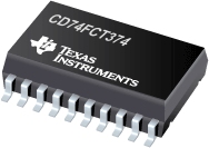
CD74FCT374 - 具有三态输出的 BiCMOS FCT 接口逻辑八路 D 类触发器
CD74FCT374是TI德州仪器公司的一款D类触发器产品,CD74FCT374是具有三态输出的 BiCMOS FCT 接口逻辑八路 D 类触发器,本站介绍了CD74FCT374的封装应用图解、特点和优点、功能等,并给出了与CD74FCT374相关的TI元器件型号供参考。
CD74FCT374 - 具有三态输出的 BiCMOS FCT 接口逻辑八路 D 类触发器 - D类触发器 - 触发器/锁存器/寄存器 - 德州仪器
The CD74FCT374 is an octal, edge-triggered, D-type flip-flop that uses a small-geometry BiCMOS technology and features 3-state outputs designed specifically for driving highly capacitive or relatively low-impedance loads. This device is particularly suitable for implementing buffer registers, I/O ports, bidirectional bus drivers, and working registers.
The output stage is a combination of bipolar and CMOS transistors that limits the output high level to two diode drops below VCC. This resultant lowering of output swing (0 V to 3.7 V) reduces power-bus ringing [a source of electromagnetic interference (EMI)] and minimizes VCC bounce and ground bounce and their effects during simultaneous output switching. The output configuration also enhances switching speed and is capable of sinking 48 mA.
The eight flip-flops enter data into their registers on the low-to-high transition of the clock (CLK). The output-enable (OE\) input controls the 3-state outputs and is independent of the register operation. When OE\ is high, the outputs are in the high-impedance state.
A buffered OE\ input can be used to place the eight outputs in either a normal logic state (high or low) or the high-impedance state. In the high-impedance state, the outputs neither load nor drive the bus lines significantly. The high-impedance state and the increased drive provide the capability to drive bus lines without interface or pullup components.
OE\ does not affect internal operations of the flip-flop. Old data can be retained or new data can be entered while the outputs are in the high-impedance state.
To ensure the high-impedance state during power up or power down, OE\ should be tied to VCC through a pullup resistor; the minimum value of the resistor is determined by the current-sinking capability of the driver.
The CD74FCT374 is characterized for operation from 0°C to 70°C.
- BiCMOS Technology With Low Quiescent Power
- 3-State Outputs Drive Bus Lines Directly
- Buffered Inputs
- Noninverted Outputs
- Input/Output Isolation From VCC
- Controlled Output Edge Rates
- 48-mA Output Sink Current
- Output Voltage Swing Limited to 3.7 V
- SCR Latch-Up-Resistant BiCMOS Process and Circuit Design
- Package Options Include Plastic Small-Outline (M) and Shrink Small-Outline (SM) Packages and Standard Plastic (E) DIP
- DAC7563T - DACxx6xT 16 位双路低功耗超低毛刺脉冲缓冲电压输出 DAC
- PTH04T230W - 6-A, 2.2V to 5.5V Input, Non-Isolated, Wide Output, Adjustable Power Module with TurboTrans
- DS42MB200 - 具有 Tx 预强调和 Rx 均衡的双路 4.25 Gbps 2:1/1:2 CML Mux/缓冲器
- SN54LVC74A-SP - 具有清零和预设功能的双路上升沿 D 类触发器
- ADS62P23 - 具有可选 DDR LVDS 或 CMOS 输出的双路 12 位 80MSPS ADC
- DRV8843 - 2.5A 双路刷式或单路双极步进电机驱动器(PWM 控制器)
- UCC3813-2 - 低功耗经济型 BiCMOS 电流模式 PWM
- SN74ACT374 - 具有三态输出的八路 D 类边沿触发器
- ADC1173 - 8 位、3 V、15MSPS、33mW A/D 转换器
- LM95221 - 采用 TruTherm 技术且具有 SMBus 和 I2C 接口的双路远程和本地温度传感器

