


- SN74LV541ADGVRE4 - 集成电路(IC) > 逻辑 > 缓冲器,驱动器,接收器,收发器
- UCC561DPTR - 集成电路(IC) > 接口 > 信号端接器
- LM48411TL/NOPB - 集成电路(IC) > 线性 > 放大器 > 音频放大器
- LM5101AM - 集成电路(IC) > 电源管理(PMIC) > 栅极驱动器
- TPS76912DBVT - 集成电路(IC) > 电源管理(PMIC) > 稳压器 - 线性
- SN74HC244QPWRQ1 - 集成电路(IC) > 逻辑 > 缓冲器,驱动器,接收器,收发器
- LMV431AIZ - 集成电路(IC) > 电源管理(PMIC) > 电压基准
- SN74LVC16244ADL - 集成电路(IC) > 逻辑 > 缓冲器,驱动器,接收器,收发器
- SN74AHCU04D - 集成电路(IC) > 逻辑 > 门和反相器
- UCC3813DTR-0 - 集成电路(IC) > 电源管理(PMIC) > DC-DC 开关控制器
- TPSM82810EVM-089 - 开发板,套件,编程器 > 评估板 > DC/DC 和 AC/DC(离线)SMPS 评估板
- TLE2237CDW - 集成电路(IC) > 线性 > 放大器 > 仪器,运算放大器,缓冲器
- TMS320C5514AZCHA10 - 集成电路(IC) > 嵌入式 > DSP(数字信号处理器)
- THS3095DDA - 集成电路(IC) > 线性 > 放大器 > 仪器,运算放大器,缓冲器
- LMV824DGVRG4 - 线性器件 - 放大器 - 仪器、运算放大器、缓冲放大器
- MAX202IN - 集成电路(IC) > 接口 > 驱动器,接收器,收发器
- LM10011EVM - 开发板,套件,编程器 > 评估板 > 评估和演示板及套件
- LM2577SX-ADJ/S5001804 - 集成电路(IC) > 电源管理(PMIC) > 稳压器 - DC-DC 开关稳压器
- SN74ABT646DGVRE4 - 逻辑 - 缓冲器,驱动器,接收器,收发器
- DS90C363MTDX/NOPB - 集成电路(IC) > 接口 > 专用


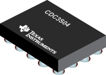
CDC3S04 - CDC3S04 Quad Sine-Wave Clock Buffer with LDO
CDC3S04是TI德州仪器公司的一款单端产品,CDC3S04是CDC3S04 Quad Sine-Wave Clock Buffer with LDO,本站介绍了CDC3S04的封装应用图解、特点和优点、功能等,并给出了与CDC3S04相关的TI元器件型号供参考。
CDC3S04 - CDC3S04 Quad Sine-Wave Clock Buffer with LDO - 单端 - 时钟缓冲器 - 德州仪器
The CDC3S04 is a four-channel low-power low-jitter sine-wave clock buffer. It can be used to buffer a single master clock to multiple peripherals. The four sine-wave outputs (CLK1–CLK4) are designed for minimal channel-to-channel skew and ultralow additive output jitter.
Each output has its own clock request inputs which enables the dedicated clock output. These clock requests are active-high (can also be changed to be active-low via I2C), and an output signal is generated that can be sent back to the master clock to request the clock (MCLK_REQ). MCKL_REQ is an open-source output and supports the wired-OR function (default mode). It needs an external pulldown resistor. MCKL_REQ can be changed to wired-AND or push-pull functionality via I2C.
The CDC3S04 also provides an I2C interface (Hs-mode) that can be used to enable or disable the outputs, select the polarity of the REQ inputs, and allow control of internal decoding.
The CDC3S04 features an on-chip high-performance LDO that accepts voltages from 2.3 V to 5.5 V and outputs a 1.8-V supply. This 1.8-V supply can be used to power an external 1.8-V TCXO. It can be enabled or disabled for power saving at the TCXO.
A low signal at the RESET input switches the outputs CLK1 and CLK4 into the default state. In this configuration, CLK1 and CLK4 are ON (see ); the remaining device function is not affected. Also, the RESET input provides a glitch filter which rejects spikes of typical 300 ns on the RESET line to preserve false reset. A complete device reset to the default condition can be initiated by a power-up cycle of VDD_DIG.
The CDC3S04 operates from two 1.8-V supplies. There is a core supply (VDD_DIG/GND_DIG) for the core logic and a low-noise analog supply (VDD_ANA/GND_ANA) for the sine-wave outputs. The CDC3S04 is designed for sequence-less power up. Both supply voltages may be applied in any order.
The CDC3S04 is offered in a 0.4-mm pitch WCSP package (1.6 mm × 2 mm) and is optimized for low standby current (0.5 µA). It is characterized for operation from –40°C to 85°C.
- 1:4 Low-Jitter Clock Buffer
- Single-Ended Sine-Wave Clock Input and Outputs
- Ultralow Phase Noise and Standby Current
- Individual Clock Request Inputs for Each Output
- On-Chip Low-Dropout Output (LDO) for Low-Noise TCXO Supply
- Serial I2C Interface (Compatible With High-Speed Mode, 3.4 Mbit/s)
- 1.8-V Device Power Supply
- Wide Temperature Range, –40°C to 85°C
- ESD Protection: 2 KV HBM, 750 V CDM, and 100 V MM
- Small 20-Pin Chip-Scale Package: 0.4-mm Pitch WCSP (1.6 mm × 2 mm)
- SN74AHC157 - 四路 2 线路至 1 线路数据选择器/多路复用器
- FDC2214 - FDC2112 FDC2114
- TS3A44159-DIE - 四路 SPDT 模拟开关 具有两个控制输入的四通道 2:1 多路复用器/多路解复用器
- SN74LVC08A-EP - 增强型产品四路 2 输入正与门
- DS3680 - 四路电话中继驱动器
- CD54ACT112 - 具有设置和复位功能的双路下降沿 J-K 触发器
- CSD23381F4 - 12-V, P-Channel NexFET? Power MOSFET, CSD23381F4
- CD4724B - CMOS 8 位可寻址锁存器
- TLV863M - 监控器和复位IC
- UC2834M - 高效率线性稳压器

