


- SN74LV164DR - 集成电路(IC) > 逻辑 > 移位寄存器
- OPA832IDR - 集成电路(IC) > 线性 > 放大器 > 视频放大器和模块
- PCF8575DGVR - 集成电路(IC) > 接口 > I/O 扩展器
- 74AC11000NSR - 集成电路(IC) > 逻辑 > 门和反相器
- SN74AHCT02PWR - 集成电路(IC) > 逻辑 > 门和反相器
- TPS79401DGNRG4 - 集成电路(IC) > 电源管理(PMIC) > 稳压器 - 线性
- TLV62585EVM-824 - 开发板,套件,编程器 > 评估板 > DC/DC 和 AC/DC(离线)SMPS 评估板
- LMH6502MAX/NOPB - 集成电路(IC) > 线性 > 放大器 > 仪器,运算放大器,缓冲器
- SN74AUC1G86DBVRE4 - 集成电路(IC) > 逻辑 > 门和反相器
- DAC102S085CIMM - 集成电路(IC) > 数据采集 > 数模转换器(DAC)
- CDCR61APWR - 集成电路(IC) > 时钟/定时 > 应用特定时钟/定时
- PDRV5053PAQLPG - 传感器,变送器 > 磁性传感器 > 线性、罗盘(IC)
- INA199C1QDCKRQ1 - 集成电路(IC) > 线性 > 放大器 > 仪器,运算放大器,缓冲器
- TRSF3243CPWG4 - 集成电路(IC) > 接口 > 驱动器,接收器,收发器
- BQ25895RTWT - 集成电路(IC) > 电源管理(PMIC) > 电池充电器
- TPS61182EVM-259 - 开发板,套件,编程器 > 评估板 > LED 驱动器评估板
- LM8365BALMF27/NOPB - 集成电路(IC) > 电源管理(PMIC) > 监控器
- OPA210IDGKT - 集成电路(IC) > 线性 > 放大器 > 仪器,运算放大器,缓冲器
- CD4044BPWR - 集成电路(IC) > 逻辑 > 锁存器
- DRV5023BIQDBZR - 传感器,变送器 > 磁性传感器 > 开关(固态)


CDCE62005 - 具有集成双路 VCO 的 5/10 路输出时钟发生器/抖动消除器
CDCE62005是TI德州仪器公司的一款低抖动(1psecRMS)产品,CDCE62005是具有集成双路 VCO 的 5/10 路输出时钟发生器/抖动消除器,本站介绍了CDCE62005的封装应用图解、特点和优点、功能等,并给出了与CDCE62005相关的TI元器件型号供参考。
CDCE62005 - 具有集成双路 VCO 的 5/10 路输出时钟发生器/抖动消除器 - 低抖动(1psecRMS) - 时钟发生器 - 德州仪器
- Superior Performance:
- Low Noise Clock Generator: 550 fs rms typical (10 kHz to 20 MHz Integration Bandwidth), FC = 100 MHz
- Low Noise Jitter Cleaner: 2.6 ps rms typical (10 kHz to 20 MHz Integration Bandwidth), FC = 100 MHz
- Flexible Frequency Planning:
- 5 Fully Configurable Outputs: LVPECL, LVDS, LVCMOS and Special High Swing Output Modes
- Unique Dual-VCO Architecture Supports a Wide Tuning Range: 1.750 GHz to 2.356 GHz
- Output Frequency Ranges from 4.25 MHz to 1.175 GHz in Synthesizer Mode
- Output Frequency up to 1.5 GHz in Fan-Out Mode
- Independent Coarse Skew Control on all Outputs
- High Flexibility:
- Integrated EEPROM Determines Device Configuration at Power-up
- Smart Input Multiplexer Automatically Switches Between One of Three Reference Inputs
- 7 × 7 mm 48-pin VQFN Package (RGZ)
- –40°C to 85°C Temperature Range
- Wireless Infrastructure
- Switches and Routers
- Medical Electronics
- Military and Aerospace
- Industrial
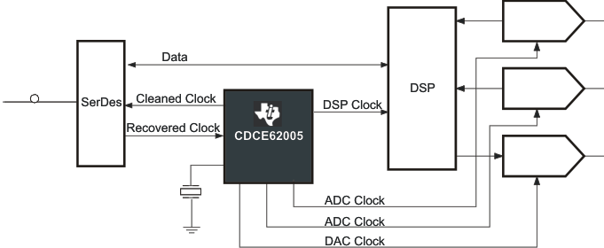
The CDCE62005 is a high performance clock generator and distributor featuring low output jitter, a high degree of configurability via a SPI interface, and programmable start up modes determined by on-chip EEPROM. Specifically tailored for clocking data converters and high-speed digital signals, the CDCE62005 achieves jitter performance well under 1 ps RMS (10 kHz to 20 MHz integration bandwidth).
The CDCE62005 incorporates a synthesizer block with partially integrated loop filter, a clock distribution block including programmable output formats, and an input block featuring an innovative smart multiplexer. The clock distribution block includes five individually programmable outputs that can be configured to provide different combinations of output formats (LVPECL, LVDS, LVCMOS). Each output can also be programmed to a unique output frequency (up to 1.5 GHz) and skew relationship via a programmable delay block (note that frequency range depends on operational mode and output format selected). If all outputs are configured in single-ended mode (for example, LVCMOS), the CDCE62005 supports up to ten outputs. Each output can select one of four clock sources to condition and distribute including any of the three clock inputs or the output of the frequency synthesizer. The input block includes two universal differential inputs which support frequencies in the range of 40 kHz to 500 MHz and an auxiliary input that can be configured to connect to an external crystal via an on chip oscillator block.
The smart input multiplexer has two modes of operation, manual and automatic. In manual mode, the user selects the synthesizer reference via the SPI interface. In automatic mode, the input multiplexer will automatically select between the highest priority input clock available.
| PART NUMBER | PACKAGE | BODY SIZE (NOM) |
|---|---|---|
| CDCE62005 | VQFN (48) | 7.00 mm × 7.00 mm |
- CDCLVP1216 - 低抖动 2 路输入可选 1:16 通用 LVPECL 缓冲器
- TPS2051C - 单通道、限流 USB 配电开关
- LM5008A - 100V、350mA 宽输入电压恒定导通时间降压开关稳压器
- CDCLVC1110 - 低抖动 1:10 LVCMOS 扇出时钟缓冲器
- DS90LV047A - 3V LVDS 四路 CMOS 差动线路驱动器
- SN74AS151 - 8 选 1 数据选择器/多路复用器
- CD74HC08-Q1 - 汽车类四路 2 输入正与门
- LMH2110 - 具有 45 dB 动态范围的 8 GHz 对数 RMS 功率检测器
- THS1206M - 12 位 6MSPS ADC,具有四通道 (配置),DSP/uP IF,集成 16x FIFO、信道自动扫描功能和低功耗模式
- TPS65050 - 2.25MHz dual step down converter with 4 low input voltage LDOs

