



- SN65MLVD205DR - 集成电路(IC) > 接口 > 驱动器,接收器,收发器
- DAC38RF82EVM - 开发板,套件,编程器 > 评估板 > 数模转换器(DAC)评估板
- BZX84WC5V6DCKRQ1 - 分立半导体产品 > 二极管 > 齐纳 > 单齐纳二极管
- OMAP5910JGVL2 - 集成电路(IC) > 嵌入式 > 微处理器
- ADC12130CIWMX/NOPB - 集成电路(IC) > 数据采集 > 模数转换器(ADC)
- SN74LVC1G17DCKRE4 - 集成电路(IC) > 逻辑 > 缓冲器,驱动器,接收器,收发器
- 78SR153VC - 板安装电源 > 直流转换器
- SN74ALVCH32244KR - 集成电路(IC) > 逻辑 > 缓冲器,驱动器,接收器,收发器
- INA240A1PWR - 集成电路(IC) > 线性 > 放大器 > 仪器,运算放大器,缓冲器
- LM4938MHX - 集成电路(IC) > 线性 > 放大器 > 音频放大器
- PTH04070WAS - 板安装电源 > 直流转换器
- SN74LV123ATPWRG4Q1 - 集成电路(IC) > 逻辑 > 多谐振荡器
- SN74HC74D - 集成电路(IC) > 逻辑 > 触发器
- MSP430FR5869IRGZT - 集成电路(IC) > 嵌入式 > 微控制器
- MSP430F415IPM - 集成电路(IC) > 嵌入式 > 微控制器
- LMH6725MA/NOPB - 集成电路(IC) > 线性 > 放大器 > 仪器,运算放大器,缓冲器
- OPT4060DTSEVM - 开发板,套件,编程器 > 评估板 > 传感器评估板
- HPA02218RTERQ1 - 电源管理IC - 稳压器 - DC DC 开关稳压器
- LP38852EVAL - 开发板,套件,编程器 > 评估板 > 线性稳压器评估板
- LM3S1621-IQC80-C5T - 集成电路(IC) > 嵌入式 > 微控制器



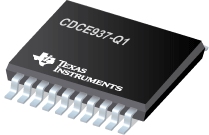
CDCE937-Q1 - 具有 2.5V 或 3.3V LVCMOS 输出的汽车类可编程 3-PLL VCXO 时钟合成器
CDCE937-Q1是TI德州仪器公司的一款无产品,CDCE937-Q1是具有 2.5V 或 3.3V LVCMOS 输出的汽车类可编程 3-PLL VCXO 时钟合成器,本站介绍了CDCE937-Q1的封装应用图解、特点和优点、功能等,并给出了与CDCE937-Q1相关的TI元器件型号供参考。
CDCE937-Q1 - 具有 2.5V 或 3.3V LVCMOS 输出的汽车类可编程 3-PLL VCXO 时钟合成器 - 无 -
CDCE937-Q1 (正在供货)
The CDCE937 and CDCEL937 are modular PLL-based low-cost high-performance programmable clock synthesizers, multipliers, and dividers. It generates up to seven output clocks from a single input frequency. Each output can be programmed in-system for any clock frequency up to 230MHz, using up to three independent configurable PLLs.
The CDCx937 has separate output supply pins, VDDOUT, which is 1.8 V for CDCEL937 and to 2.5 V to 3.3 V for CDCE937.
The input accepts an external crystal or LVCMOS clock signal. If an external crystal is used, an on-chip load capacitor is adequate for most applications. The value of the load capacitor is programmable from 0 to 20pF. Additionally, an on-chip VCXO is selectable which allows synchronization of the output frequency to an external control signal, that is, PWM signal.
The deep M/N divider ratio allows the generation of zero ppm audio/video, networking (WLAN, BlueTooth, Ethernet, GPS) or Interface (USB, IEEE1394, Memory Stick) clocks from a reference input frequency such as 27MHz.
All PLLs supports SSC (Spread-Spectrum Clocking). SSC can be Center-Spread or Down-Spread clocking which is a common technique to reduce electro-magnetic interference (EMI).
Based on the PLL frequency and the divider settings, the internal loop filter components are automatically adjusted to achieve high stability and optimized jitter transfer characteristic of each PLL.
The device supports non-volatile EEPROM programming for ease-customized application. It is preset to a factory default configuration (see the Default Device Configuration section). It can be reprogrammed to a different application configuration before PCB assembly, or reprogrammed by in-system programming. All device settings are programmable through SDA/SCL bus, a 2-wire serial interface.
Three programmable control inputs, S0, S1 and S2, can be used to control various aspects of operation including frequency selection changing the SSC parameters to lower EMI, PLL bypass, power down, and choosing between low level or 3-state for output-disable function.
The CDCEx937 operates in 1.8-V environment. It is characterized for operation from –40°C to 125°C.
- Qualified for Automotive Applications
- Member of Programmable Clock Generator Family
- CDCE913/CDCEL913: 1-PLL, 3 Outputs
- CDCE925/CDCEL925: 2-PLL, 5 Outputs
- CDCE937/CDCEL937: 3-PLL, 7 Outputs
- CDCE949/CDCEL949: 4-PLL, 9 Outputs
- In-System Programmability and EEPROM
- Serial Programmable Volatile Register
- Nonvolatile EEPROM to Store Customer Setting
- Flexible Input Clocking Concept
- External Crystal: 8 MHz to 32 MHz
- On-Chip VCXO: Pull Range ±150 ppm
- Single-Ended LVCMOS up to 160 MHz
- Selectable Output Frequency up to 230 MHz
- Low-Noise PLL Core
- Integrated PLL Loop Filter Components
- Low Period Jitter (Typ 60 ps)
- Separate Output Supply Pins
- CDCE937: 3.3 V and 2.5 V
- CDCEL937: 1.8 V
- 1.8-V Device Power Supply
- Flexible Clock Driver
- Three User-Definable Control Inputs [S0/S1/S2]; e.g., SSC Selection, Frequency Switching, Output Enable or Power Down
- Generates Highly Accurate Clocks for Video, Audio, USB, IEEE1394, RFID, Bluetooth, WLAN, Ethernet, and GPS
- Generates Common Clock Frequencies Used With TI DaVinci, OMAP, DSPs
- Programmable SSC Modulation
- Enables 0-PPM Clock Generation
- Latch-Up Performance Meets 100 mA Per JESD 78, Class I
- Wide Temperature Range –40° C to 125° C
- Packaged in TSSOP
- Development and Programming Kit for Easy PLL Design
- APPLICATIONS
- D-TV, HD-TV, STB, IP-STB, DVD-Player, DVD-Recorder, Printer
- UCC2897A - 高级电流模式有源钳位 PWM 控制器
- TLVH432 - 低电压可调节精密并联稳压器
- TPS65142 - 用于具有 6ch WLED 驱动器的 LCD 面板的 LCD 偏置解决方案
- TS3L301 - 具有低而平坦的导通电阻的 16 位到 8 位 SPDT 千兆 LAN 交换机
- TS5A23157-Q1 - 汽车类双路 15Ω SPDT 模拟开关
- LM4040B20 - 2.048V 精密微功耗并联电压参考,0.2% 精确度
- SN75C185 - 低功耗多路驱动器和接收器
- REF3133 - 采用 SOT23-3 封装最大漂移 20ppm/℃ 静态电流 100μA 的电压参考系列
- TMS320F28375D - TMS320F2837xD 双核 Delfino 微控制器
- REF3240 - 采用 SOT23-6 封装的 4.096V 输出 4ppm/C 漂移 100uA 系列(带隙)电压参考

