


- LM6584MT - 集成电路(IC) > 线性 > 放大器 > 视频放大器和模块
- LMK04808BEVAL/NOPB - 开发板,套件,编程器 > 评估板 > 评估和演示板及套件
- LM60440ARPKR - 集成电路(IC) > 电源管理(PMIC) > 稳压器 - DC-DC 开关稳压器
- LMC6044AIM - 集成电路(IC) > 线性 > 放大器 > 仪器,运算放大器,缓冲器
- MSP430P313IDL - 集成电路(IC) > 嵌入式 > 微控制器
- PCM2900E - 集成电路(IC) > 接口 > 编解码器
- LM3352MTCX-3.0 - 电源管理IC - 稳压器 - DC DC 开关稳压器
- ADS1110A1IDBVRG4 - 集成电路(IC) > 数据采集 > 模数转换器(ADC)
- ONET2511PARGT - 集成电路(IC) > 线性 > 放大器 > 仪器,运算放大器,缓冲器
- SN74LS266DRE4 - 集成电路(IC) > 逻辑 > 门和反相器
- TLC3702CDR - 集成电路(IC) > 线性 > 比较器
- CD74HC4040M96 - 集成电路(IC) > 逻辑 > 计数器,除法器
- SN74BCT244NSR - 集成电路(IC) > 逻辑 > 缓冲器,驱动器,接收器,收发器
- TPSM8287A15BBHEVM - 开发板,套件,编程器 > 评估板 > DC/DC 和 AC/DC(离线)SMPS 评估板
- SN74LVC374ADBR - 集成电路(IC) > 逻辑 > 触发器
- LM3647IM - 集成电路(IC) > 电源管理(PMIC) > 电池充电器
- SN74LVC1G132DBVTG4 - 集成电路(IC) > 逻辑 > 门和反相器
- SN74ABT16652DL - 集成电路(IC) > 逻辑 > 缓冲器,驱动器,接收器,收发器
- NE5534ADRE4 - 线性器件 - 放大器 - 仪器、运算放大器、缓冲放大器
- TPS2411RMSR - 集成电路(IC) > 电源管理(PMIC) > OR 控制器,理想二极管


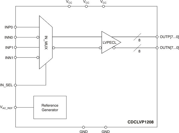
CDCLVP1208 - 低抖动 2 路输入可选 1:8 通用 LVPECL 缓冲器
CDCLVP1208是TI德州仪器公司的一款差动产品,CDCLVP1208是低抖动 2 路输入可选 1:8 通用 LVPECL 缓冲器,本站介绍了CDCLVP1208的封装应用图解、特点和优点、功能等,并给出了与CDCLVP1208相关的TI元器件型号供参考。
CDCLVP1208 - 低抖动 2 路输入可选 1:8 通用 LVPECL 缓冲器 - 差动 - 时钟缓冲器 - 德州仪器
- 2:8 Differential Buffer
- Selectable Clock Inputs Through Control terminal
- Universal Inputs Accept LVPECL, LVDS, and LVCMOS/LVTTL
- Eight LVPECL Outputs
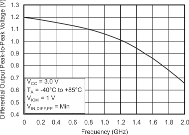
- Maximum Clock Frequency: 2 GHz
- Maximum Core Current Consumption: 73 mA
- Very Low Additive Jitter: <100 fs,rms in 10 kHz to 20 MHz Offset Range:
- 57 fs, rms (typical) at 122.88 MHz
- 48 fs, rms (typical) at 156.25 MHz
- 30 fs, rms (typical) at 312.5 MHz
- 2.375-V to 3.6-V Device Power Supply
- Maximum Propagation Delay: 450 ps
- Maximum Output Skew: 20 ps
- LVPECL Reference Voltage, VAC_REF, Available for Capacitive-Coupled Inputs
- Industrial Temperature Range: –40°C to 85°C
- Supports 105°C PCB Temperature (Measured with a Thermal Pad)
- ESD Protection Exceeds 2 kV (HBM)
- Available in 5-mm × 5-mm QFN-28 (RHD) Package
- Wireless Communications
- Telecommunications/Networking
- Medical Imaging
- Test and Measurement Equipment
The CDCLVP1208 is a highly versatile, low additive jitter buffer that can generate eight copies of LVPECL clock outputs from one of two selectable LVPECL, LVDS, or LVCMOS inputs for a variety of communication applications. It has a maximum clock frequency up to 2 GHz. The CDCLVP1208 features an on-chip multiplexer (MUX) for selecting one of two inputs that can be easily configured solely through a control terminal. The overall additive jitter performance is less than 0.1 ps, RMS from 10 kHz to 20 MHz, and overall output skew is as low as 20 ps, making the device a perfect choice for use in demanding applications.
The CDCLVP1208 clock buffer distributes one of two selectable clock inputs (IN0, IN1) to eight pairs of differential LVPECL clock outputs (OUT0, OUT7) with minimum skew for clock distribution. The CDCLVP1208 can accept two clock sources into an input multiplexer. The inputs can be LVPECL, LVDS, or LVCMOS/LVTTL.
The CDCLVP1208 is specifically designed for driving 50-Ω transmission lines. When driving the inputs in single-ended mode, the LVPECL bias voltage (VAC_REF) should be applied to the unused negative input terminal. However, for high-speed performance up to 2 GHz, differential mode is strongly recommended.
The CDCLVP1208 is packaged in a small 28-pin, 5-mm x 5-mm QFN package and is characterized for operation from –40°C to 85°C.
| PART NUMBER | PACKAGE | BODY SIZE (NOM) |
|---|---|---|
| CDCLVP1208 | QFN (28) | 5.00 mm x 5.00 mm |
- TPS51513 - Single Phase, D-CAP+TM Synchronous Buck Controller
- DAC8311 - 采用 SC70 封装的 14 位、单通道、80uA、2.0V-5.5V DAC
- TPS22946 - 5.5V,0.2A,300mΩ 可选限流负载开关
- DS90UR241 - 5-43MHz DC 平衡 24 位 FPD 链接 II 串行器
- DRV8302 - 具有双路电流感应放大器和降压转换器的三相无刷电机前 置驱动器(PWM 控制器)
- CSD22202W15 - P 通道 NexFET 功率 MOSFET,CSD22202W15
- MSP430F67781A - MSP430F677x1A、MSP430F677x 1A、MSP430F677x1A 混合信号微控制器
- SN74AHCT08 - 四路 2 输入正与门
- TL750M05-Q1 - 低压降稳压器
- PTH08T260W - 采用 TurboTrans 技术的 3A、4.5V 至 14V 输入的非隔离宽输出可调节电源模块

