


- TP3403V/NOPB - 集成电路(IC) > 接口 > 电信
- SN74AHC04QDRQ1 - 集成电路(IC) > 逻辑 > 门和反相器
- TCAN1051HGDRQ1 - 集成电路(IC) > 接口 > 驱动器,接收器,收发器
- LP324M/NOPB - 集成电路(IC) > 线性 > 放大器 > 仪器,运算放大器,缓冲器
- TMS320C6454BCTZ8 - 集成电路(IC) > 嵌入式 > DSP(数字信号处理器)
- TPS2491DGS - 集成电路(IC) > 电源管理(PMIC) > 热插拔控制器
- TPS76330QDBVRQ1 - 集成电路(IC) > 电源管理(PMIC) > 稳压器 - 线性
- XTR106U/2K5 - 集成电路(IC) > 接口 > 传感器和检测器接口
- UCC27201ADDA - 集成电路(IC) > 电源管理(PMIC) > 栅极驱动器
- TS5USBC412YFFR - 集成电路(IC) > 接口 > 模拟开关 - 特殊用途
- LM20144QMH/NOPB - 集成电路(IC) > 电源管理(PMIC) > 稳压器 - DC-DC 开关稳压器
- PCA9535PW - 集成电路(IC) > 接口 > I/O 扩展器
- LM741H - 集成电路(IC) > 线性 > 放大器 > 仪器,运算放大器,缓冲器
- ISO7521CDW - 隔离器 > 数字隔离器
- LM341T-5.0 - 集成电路(IC) > 电源管理(PMIC) > 稳压器 - 线性
- LM4140ACMX-4.1 - 集成电路(IC) > 电源管理(PMIC) > 电压基准
- LM95231BIMMX-1 - 传感器,变送器 > 温度传感器 > 模拟和数字输出
- LM2586SX-3.3/NOPB - 集成电路(IC) > 电源管理(PMIC) > 稳压器 - DC-DC 开关稳压器
- LMH6502MA/NOPB - 集成电路(IC) > 线性 > 放大器 > 仪器,运算放大器,缓冲器
- DAC8560IBDGKR - 集成电路(IC) > 数据采集 > 数模转换器(DAC)


CDCLVP1212 - 低抖动 2 路输入可选 1:12 通用 LVPECL 缓冲器
CDCLVP1212是TI德州仪器公司的一款差动产品,CDCLVP1212是低抖动 2 路输入可选 1:12 通用 LVPECL 缓冲器,本站介绍了CDCLVP1212的封装应用图解、特点和优点、功能等,并给出了与CDCLVP1212相关的TI元器件型号供参考。
CDCLVP1212 - 低抖动 2 路输入可选 1:12 通用 LVPECL 缓冲器 - 差动 - 时钟缓冲器 - 德州仪器
- 2:12 Differential Buffer
- Selectable Clock Inputs Through Control Terminal
- Universal Inputs Accept LVPECL, LVDS, and LVCMOS/LVTTL
- 12 LVPECL Outputs
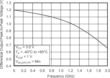
- Maximum Clock Frequency: 2 GHz
- Maximum Core Current Consumption: 88 mA
- Very Low Additive Jitter: <100 fs, rms in 10-kHz to 20-MHz Offset Range:
- 57 fs, rms (typ) @ 122.88 MHz
- 48 fs, rms (typ) @ 156.25 MHz
- 30 fs, rms (typ) @ 312.5 MHz
- 2.375-V to 3.6-V Device Power Supply
- Maximum Propagation Delay: 550 ps
- Maximum Output Skew: 25 ps
- LVPECL Reference Voltage, VAC_REF, Available for Capacitive-Coupled Inputs
- Industrial Temperature Range: –40°C to 85°C
- ESD Protection Exceeds 2 kV (HBM)
- Supports 105°C PCB Temperature (Measured with a Thermal Pad)
- Available in 6-mm × 6-mm QFN-40 (RHA) Package
- Wireless Communications
- Telecommunications/Networking
- Medical Imaging
- Test and Measurement Equipment
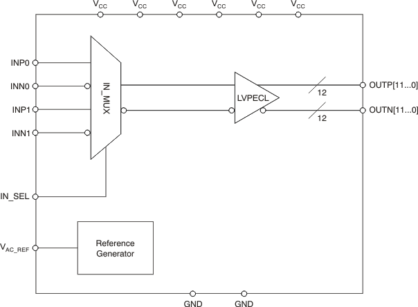
The CDCLVP1212 is a highly versatile, low additive jitter buffer that can generate 12 copies of LVPECL clock outputs from one of two selectable LVPECL, LVDS, or LVCMOS inputs for a variety of communication applications. It has a maximum clock frequency up to 2 GHz. The CDCLVP1212 features an on-chip multiplexer (MUX) for selecting one of two inputs that can be easily configured solely through a control terminal. The overall additive jitter performance is less than 0.1 ps, RMS from 10 kHz to 20 MHz, and overall output skew is as low as 25 ps, making the device a perfect choice for use in demanding applications.
The CDCLVP1212 clock buffer distributes one of two selectable clock inputs (IN0, IN1) to 12 pairs of differential LVPECL clock outputs (OUT0, OUT11) with minimum skew for clock distribution. The CDCLVP1212 can accept two clock sources into an input multiplexer. The inputs can be LVPECL, LVDS, or LVCMOS/LVTTL.
The CDCLVP1212 is specifically designed for driving 50-Ω transmission lines. When driving the inputs in single-ended mode, the LVPECL bias voltage (VAC_REF) should be applied to the unused negative input terminal. However, for high-speed performance up to 2 GHz, differential mode is strongly recommended.
The CDCLVP1212 is packaged in a small 40-terminal, 6-mm x 6-mm QFN package and is characterized for operation from –40°C to 85°C.
| PART NUMBER | PACKAGE | BODY SIZE (NOM) |
|---|---|---|
| CDCLVP1212 | QFN (40) | 6.00 mm x 6.00 mm |
- UCC2803 - 低功耗 BiCMOS 电流模式 PWM
- ISO7420 - 低功耗双通道隔离器
- SM320C6711D-EP - 增强型产品浮点 DSP
- LP5560 - 具有单线制接口的可编程 LED 驱动器
- SN74CBTLV1G125-Q1 - 汽车类低电压单路 FET 总线开关
- ADC3242 - 双通道 14 位 125 Msps 模数转换器
- SN74ALS323 - 具有同步清零功能和三态输出的 8 位通用移位/存储寄存器
- MSP430F5506 - 混合信号微处理器
- TMS320F28375D - TMS320F2837xD 双核 Delfino 微控制器
- TMP122-EP - 增强型产品,具有 SPI 接口的 ±1°C 温度传感器,支持报警功能

