


- TPS77601DG4 - 集成电路(IC) > 电源管理(PMIC) > 稳压器 - 线性
- SN74AHC02DBR - 集成电路(IC) > 逻辑 > 门和反相器
- MSP430FR5989IRGCT - 集成电路(IC) > 嵌入式 > 微控制器
- INA296B5IDGKR - 集成电路(IC) > 线性 > 放大器 > 仪器,运算放大器,缓冲器
- SN65C3232EDWR - 集成电路(IC) > 接口 > 驱动器,接收器,收发器
- PT4583N - 板安装电源 > 直流转换器
- ADS4122IRGZT - 集成电路(IC) > 数据采集 > 模数转换器(ADC)
- SN74F2373N - 集成电路(IC) > 逻辑 > 锁存器
- BQ24150YFFT - 集成电路(IC) > 电源管理(PMIC) > 电池充电器
- SN74HC151ANSR - 集成电路(IC) > 逻辑 > 信号开关,多路复用器,解码器
- LM393ADR - 集成电路(IC) > 线性 > 比较器
- BQ2945SN-C409 - 集成电路(IC) > 电源管理(PMIC) > 电池管理
- TPA2005D1DGN - 集成电路(IC) > 线性 > 放大器 > 音频放大器
- TAS5719PHP - 集成电路(IC) > 线性 > 放大器 > 音频放大器
- CD40257BNSRG4 - 逻辑 - 信号开关,多路复用器,解码器
- RM46L440CPGET - 集成电路(IC) > 嵌入式 > 微控制器
- TLC271BIDG4 - 集成电路(IC) > 线性 > 放大器 > 仪器,运算放大器,缓冲器
- OPA4132UA - 集成电路(IC) > 线性 > 放大器 > 仪器,运算放大器,缓冲器
- CY29FCT520ATSOCTE4 - 逻辑 - 移位寄存器
- LP3882ESX-1.2/NOPB - 集成电路(IC) > 电源管理(PMIC) > 稳压器 - 线性


CDCLVP1216 - 低抖动 2 路输入可选 1:16 通用 LVPECL 缓冲器
CDCLVP1216是TI德州仪器公司的一款差动产品,CDCLVP1216是低抖动 2 路输入可选 1:16 通用 LVPECL 缓冲器,本站介绍了CDCLVP1216的封装应用图解、特点和优点、功能等,并给出了与CDCLVP1216相关的TI元器件型号供参考。
CDCLVP1216 - 低抖动 2 路输入可选 1:16 通用 LVPECL 缓冲器 - 差动 - 时钟缓冲器 - 德州仪器
- 2:16 Differential Buffer
- Selectable Clock Inputs Through Control Pin
- Universal Inputs Accept LVPECL, LVDS, and LVCMOS/LVTTL
- 16 LVPECL Outputs
- Maximum Clock Frequency: 2 GHz
- Maximum Core Current Consumption: 110 mA
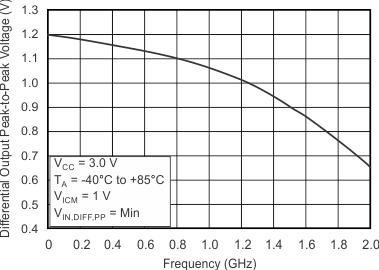
- Very Low Additive Jitter: <100 fs,rms in 10-kHz to 20-MHz Offset Range:
- 57 fs, rms (typ) @ 122.88 MHz
- 48 fs, rms (typ) @ 156.25 MHz
- 30 fs, rms (typ) @ 312.5 MHz
- 2.375 V to 3.6 V Device Power Supply
- Maximum Propagation Delay: 550 ps
- Maximum Output Skew: 30 ps
- LVPECL Reference Voltage, VAC_REF, Available for Capacitive-Coupled Inputs
- Industrial Temperature Range: –40°C to 85°C
- Supports 105°C PCB Temperature (Measured with a Thermal Pad)
- ESD Protection Exceeds 2 kV (HBM)
- Available in 7-mm × 7-mm QFN-48 (RGZ) Package
- Wireless Communications
- Telecommunications/Networking
- Medical Imaging
- Test and Measurement Equipment
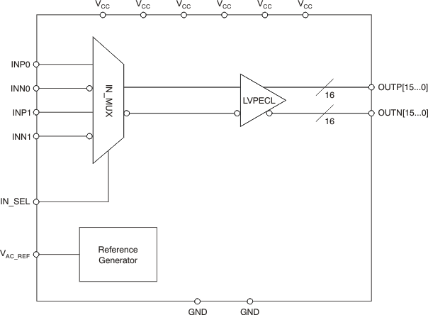
The CDCLVP1216 is a highly versatile, low additive jitter buffer that can generate 16 copies of LVPECL clock outputs from one of two selectable LVPECL, LVDS, or LVCMOS inputs for a variety of communication applications. It has a maximum clock frequency up to 2 GHz. The CDCLVP1216 features an on-chip multiplexer (MUX) for selecting one of two inputs that can be easily configured solely through a control pin. The overall additive jitter performance is less than 0.1 ps, RMS from 10 kHz to 20 MHz, and overall output skew is as low as 30 ps, making the device a perfect choice for use in demanding applications.
The CDCLVP1216 clock buffer distributes one of two selectable clock inputs (IN0, IN1) to 16 pairs of differential LVPECL clock outputs (OUT0, OUT15) with minimum skew for clock distribution. The CDCLVP1216 can accept two clock sources into an input multiplexer. The inputs can be LVPECL, LVDS, or LVCMOS/LVTTL.
The CDCLVP1216 is specifically designed for driving 50-Ω transmission lines. When driving the inputs in single-ended mode, the LVPECL bias voltage (VAC_REF) should be applied to the unused negative input pin. However, for high-speed performance up to 2 GHz, differential mode is strongly recommended.
The CDCLVP1216 is packaged in a small 48-pin, 7-mm x 7-mm QFN package and is characterized for operation from –40°C to 85°C.
| ORDER NUMBER | PACKAGE | BODY SIZE (NOM) |
|---|---|---|
| CDCLVP1216 | QFN (48) | 7.00 mm x 7.00 mm |
- TPS74801-Q1 - 汽车类单路输出 LDO、1.5A、可调节 (0.8 至 3.6V)可编程软启动
- LM3450 - 具有有源功率因数校正和相位明暗调节解码器的 LED 驱动器
- SN74LVC573A - 具有三态输出的八路透明 D 类锁存器
- LMX2581E - LMX2581E 具有集成 VCO 的宽带频率合成器
- TPS7A88 - 双通道 1A 低噪声 LDO
- TPS62160 - 采用 2x2 QFN 封装的 3-17V 1A 降压转换器
- 66AK2H14 - 多核 DSP+ARM KeyStone II 片上系统 (SoC)
- SN65HVD55 - 带使能信号的高输出全双工 RS-485 驱动器和接收器
- CSD87381P - 同步降压 NexFETTM 电源块,CSD87381P
- MSP430F6769 - MSP430F677x、MSP430F676x、M SP430F674x 混合信号微处理器

