



- MSP430F6736AIPNR - 集成电路(IC) > 嵌入式 > 微控制器
- SN74ALS74ANSR - 集成电路(IC) > 逻辑 > 触发器
- TL7705ACD - 集成电路(IC) > 电源管理(PMIC) > 监控器
- SN64BCT244DWRG4 - 集成电路(IC) > 逻辑 > 缓冲器,驱动器,接收器,收发器
- CD4502BM - 集成电路(IC) > 逻辑 > 缓冲器,驱动器,接收器,收发器
- LP3991TLX-1.8/NOPB - 集成电路(IC) > 电源管理(PMIC) > 稳压器 - 线性
- CD74HC238M96E4 - 集成电路(IC) > 逻辑 > 信号开关,多路复用器,解码器
- ADS7816EB/250 - 集成电路(IC) > 数据采集 > 模数转换器(ADC)
- LM87CIMTX - 集成电路(IC) > 电源管理(PMIC) > 热管理
- UCC27532DBVT - 集成电路(IC) > 电源管理(PMIC) > 栅极驱动器
- LM2587S-3.3 - 集成电路(IC) > 电源管理(PMIC) > 稳压器 - DC-DC 开关稳压器
- ULN2003AD - 分立半导体产品 > 晶体管 > 双极(BJT) > 双极晶体管阵列
- SN74LVCH16541ADGG - 集成电路(IC) > 逻辑 > 缓冲器,驱动器,接收器,收发器
- TPS62102EVM - 开发板,套件,编程器 > 评估板 > DC/DC 和 AC/DC(离线)SMPS 评估板
- TLC1543QFN - 集成电路(IC) > 数据采集 > 模数转换器(ADC)
- TPS658642ZQZR - 电源管理IC - 电源管理 - 专用型
- TPS92520EVM-133 - 开发板,套件,编程器 > 评估板 > LED 驱动器评估板
- LP3917RL-NL/NOPB - 集成电路(IC) > 电源管理(PMIC) > 电源管理 - 专用
- SN74AHC1G04DCKT - 集成电路(IC) > 逻辑 > 门和反相器
- TPS2110APW - 集成电路(IC) > 电源管理(PMIC) > OR 控制器,理想二极管



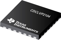
CDCLVP2104 - 低抖动双路 1:4 通用 LVPECL 缓冲器
CDCLVP2104是TI德州仪器公司的一款差动产品,CDCLVP2104是低抖动双路 1:4 通用 LVPECL 缓冲器,本站介绍了CDCLVP2104的封装应用图解、特点和优点、功能等,并给出了与CDCLVP2104相关的TI元器件型号供参考。
CDCLVP2104 - 低抖动双路 1:4 通用 LVPECL 缓冲器 - 差动 - 时钟缓冲器 - 德州仪器
The CDCLVP2104 is a highly versatile, low additive jitter buffer that can generate eight copies of LVPECL clock outputs from two LVPECL, LVDS, or LVCMOS inputs for a variety of communication applications. It has a maximum clock frequency up to 2 GHz. Each buffer block consists of one input that feeds two LVPECL outputs. The overall additive jitter performance is less than 0.1 ps, RMS from 10 kHz to 20 MHz, and overall output skew is as low as 15 ps, making the device a perfect choice for use in demanding applications.
The CDCLVP2104 clock buffer distributes two clock inputs (IN0, IN1) to eight pairs of differential LVPECL clock outputs (OUT0, OUT7) with minimum skew for clock distribution. Each buffer block consists of one input that feeds two LVPECL clock outputs. The inputs can be LVPECL, LVDS, or LVCMOS/LVTTL.
The CDCLVP2104 is specifically designed for driving 50-Ω transmission lines. When driving the inputs in single-ended mode, the LVPECL bias voltage (VAC_REF) should be applied to the unused negative input pin. However, for high-speed performance up to 2 GHz, differential mode is strongly recommended.
The CDCLVP2104 is characterized for operation from –40°C to +85°C and is available in a QFN-28, 5-mm × 5-mm package.
- Dual 1:4 Differential Buffer
- Two Clock Inputs
- Universal Inputs Can Accept LVPECL, LVDS, LVCMOS/LVTTL
- Eight LVPECL Outputs
- Maximum Clock Frequency: 2 GHz
- Maximum Core Current Consumption: 78 mA
- Very Low Additive Jitter: <100 fs, rms in 10-kHz to 20-MHz Offset Range
- 2.375 V to 3.6 V Device Power Supply
- Maximum Propagation Delay: 450 ps
- Maximum 15 ps Within Bank Output Skew
- LVPECL Reference Voltage, VAC_REF, Available for Capacitive-Coupled Inputs
- Industrial Temperature Range: –40°C to +85°C
- Available in 5-mm × 5-mm QFN-28 (RHD) Package
- ESD Protection Exceeds 2 kV (HBM)
- DLPA3000 - 用于 DLP3010 (0.3 720p) DMD 的 PMIC/LED 驱动器
- TPS63024 - TPS63024 最高效率 1A 单电感降压/升压转换器
- CD4510B - CMOS 可预设置的 BCD 加/减计数器
- LP3981 - 微功耗,300mA 超低压降 CMOS 电压稳压器
- TPS2065 - 单个 1A 限流配电开关,用于 USB 应用领域
- TMP123 - 具有 SPI 接口的 ±1°C 温度传感器
- LM25069 - 正低电压功率限制热插拔控制器
- THS5661A - 12 位、125MSPS、CommsDAC、差动 介于 2mA 至 20mA 的可变电流输出
- DAC5672A - Dual 14-Bit 275 MSPS Digital-to-Analog Converter
- SN74ABTH32501 - 具有三态输出的 36 位通用总线收发器

