


- TPS3824-25DBVR - 集成电路(IC) > 电源管理(PMIC) > 监控器
- ISO1211D - 集成电路(IC) > 接口 > 专用
- SN74ABT16821DL - 集成电路(IC) > 逻辑 > 触发器
- 5962-9451301MPA - 集成电路(IC) > 电源管理(PMIC) > DC-DC 开关控制器
- SN74LVC32AQDREP - 集成电路(IC) > 逻辑 > 门和反相器
- TPS3823-33DBVT - 集成电路(IC) > 电源管理(PMIC) > 监控器
- TLC2262IDR - 集成电路(IC) > 线性 > 放大器 > 仪器,运算放大器,缓冲器
- TRPGR30ATGB - 射频和无线 > RFID 应答器、标签
- SN65LVDS96DGG - 集成电路(IC) > 接口 > 串行器,解串器
- UCC2895DWG4 - 集成电路(IC) > 电源管理(PMIC) > DC-DC 开关控制器
- TPS62404DRCT - 集成电路(IC) > 电源管理(PMIC) > 稳压器 - DC-DC 开关稳压器
- LM386N-4 - 集成电路(IC) > 线性 > 放大器 > 音频放大器
- LMC6762AIMX/NOPB - 集成电路(IC) > 线性 > 比较器
- TL431BIDBZT - 集成电路(IC) > 电源管理(PMIC) > 电压基准
- SN74LS348DRG4 - 逻辑 - 信号开关,多路复用器,解码器
- SN74AHC04QPWR - 集成电路(IC) > 逻辑 > 门和反相器
- DS14C89AMX/NOPB - 集成电路(IC) > 接口 > 驱动器,接收器,收发器
- TPS25830AQWRHBRQ1 - 集成电路(IC) > 电源管理(PMIC) > 电源管理 - 专用
- ADS7953SBDBTR - 集成电路(IC) > 数据采集 > 模数转换器(ADC)
- PT5110C - 板安装电源 > 直流转换器


CDCM1802 - 具有可编程除法器和 LVPECL I/O + addl LVCMOS 输出的时钟缓冲器
CDCM1802是TI德州仪器公司的一款分频器产品,CDCM1802是具有可编程除法器和 LVPECL I/O + addl LVCMOS 输出的时钟缓冲器,本站介绍了CDCM1802的封装应用图解、特点和优点、功能等,并给出了与CDCM1802相关的TI元器件型号供参考。
CDCM1802 - 具有可编程除法器和 LVPECL I/O + addl LVCMOS 输出的时钟缓冲器 - 分频器 - 时钟缓冲器 - 德州仪器
- Distributes One Differential Clock Input to One LVPECL Differential Clock Output and One LVCMOS Single-Ended Output
- Programmable Output Divider for Both LVPECL and LVCMOS Outputs
- 1.6-ns Output Skew Between LVCMOS and LVPECL Transitions Minimizing Noise
- 3.3-V Power Supply (2.5-V Functional)
- Signaling Rate Up to 800-MHz LVPECL and 200-MHz LVCMOS
- Differential Input Stage for Wide Common-Mode Range Also Provides VBB Bias Voltage Output for Single-Ended Input Signals
- Receiver Input Threshold ±75 mV
- 16-Pin VQFN Package (3.00 mm × 3.00 mm)
- Networking and Data Communications
- Medical Imaging
- Portable Test and Measurement
- High-end A/V
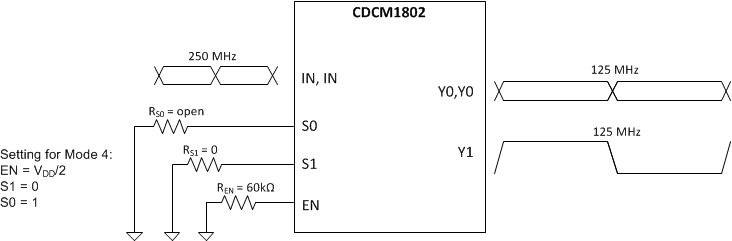
The CDCM1802 clock driver distributes one pair of differential clock input to one LVPECL differential clock output pair, Y0 and Y0, and one single-ended LVCMOS output, Y1. It is specifically designed for driving 50-Ω transmission lines. The LVCMOS output is delayed by 1.6 ns over the PECL output stage to minimize noise impact during signal transitions.
The CDCM1802 has two control pins, S0 and S1, to select different output mode settings. The S[1:0] pins are 3-level inputs. Additionally, an enable pin EN is provided to disable or enable all outputs simultaneously. The CDCM1802 is characterized for operation from −40°C to 85°C.
For single-ended driver applications, the CDCM1802 provides a VBB output pin that can be directly connected to the unused input as a common-mode voltage reference.
| PART NUMBER | PACKAGE | BODY SIZE (NOM) |
|---|---|---|
| CDCM1802 | VQFN (16) | 3.00 mm × 3.00 mm |
- TPS65800 - 集成单节锂离子电池和电源管理 IC (PMIC)
- TMS570LS3135 - 16/32-Bit RISC Flash Microcontroller
- SN65HVDA540 - 具有 I/O 电平转换和电源优化的汽车类 5V CAN 收发器
- SN75182 - 双路差动线路接收器
- CSD18537NKCS - 60V,N 通道 NexFET 功率 MOSFET
- MSP430AFE233 - 16 位超低功耗微处理器,具有 8kB 闪存、512B RAM 和 3 段 SD24
- LMX2541 - 具有集成 VCO 的超低噪声 PLLatinum 频率合成器
- LP2950-50 - Fixed 5V Micropower Voltage Regulator with Shutdown
- SN54166 - 并联负载 8 位移位寄存器
- CD54HC4052 - 高速 CMOS 逻辑模拟多路复用器/多路解复用器

