


- TPA2028D1YZFEVM - 开发板,套件,编程器 > 评估板 > 音频放大器评估板
- MSP430F5436IPZ - 集成电路(IC) > 嵌入式 > 微控制器
- LMR23630EVM - 开发板,套件,编程器 > 评估板 > DC/DC 和 AC/DC(离线)SMPS 评估板
- SN74LVT16835DLR - 集成电路(IC) > 逻辑 > 通用总线功能
- REF4132A25DBVRQ1 - 集成电路(IC) > 电源管理(PMIC) > 电压基准
- TIOS102DRCR - 集成电路(IC) > 接口 > 传感器和检测器接口
- LM3706XQBP-308 - 集成电路(IC) > 电源管理(PMIC) > 监控器
- DS92LX2121SQX/NOPB - 集成电路(IC) > 接口 > 串行器,解串器
- MSP430FE425IPMR - 集成电路(IC) > 嵌入式 > 微控制器
- LP3995ILD-1.8 - 集成电路(IC) > 电源管理(PMIC) > 稳压器 - 线性
- LM95231EVAL - 评估板 - 传感器
- LM358ADE4 - 集成电路(IC) > 线性 > 放大器 > 仪器,运算放大器,缓冲器
- SN54ALS273J - 集成电路(IC) > 逻辑 > 触发器
- SN74LVC574ARGYR - 集成电路(IC) > 逻辑 > 触发器
- CD4515BM - 集成电路(IC) > 逻辑 > 信号开关,多路复用器,解码器
- TMDSILPFCKIT - 开发板,套件,编程器 > 评估板 > 评估和演示板及套件
- SN74ALVCH16863DL - 集成电路(IC) > 逻辑 > 缓冲器,驱动器,接收器,收发器
- TL750M05CKCSE3 - 集成电路(IC) > 电源管理(PMIC) > 稳压器 - 线性
- PT5045L - 直流转换器
- BQ24079TEVM - 开发板,套件,编程器 > 评估板 > 评估和演示板及套件


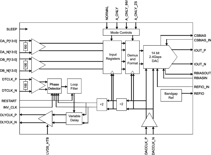
DAC5670-SP - 14 位 2.4GSPS 数模转换器
DAC5670-SP是TI德州仪器公司的一款高速DAC(>10MSPS)产品,DAC5670-SP是14 位 2.4GSPS 数模转换器,本站介绍了DAC5670-SP的封装应用图解、特点和优点、功能等,并给出了与DAC5670-SP相关的TI元器件型号供参考。
DAC5670-SP - 14 位 2.4GSPS 数模转换器 - 高速DAC(>10MSPS) - 数模转换器 - 德州仪器
- 14-Bit Resolution
- 2.4-GSPS Max Update Rate DAC
- Dual Differential Input Ports
- Even/Odd Demultiplexed Data
- Maximum 1.2 GSPS Each Port, 2.4 GSPS Total
- Dual 14-Bit Inputs + 1 Reference Bit
- DDR Output Clock
- DLL Optimized Clock Timing Synchronized to Reference Bit
- LVDS and HyperTransport™ Voltage Level Compatible
- Internal 100-Ω Terminations for Data and Reference Bit Inputs
- Selectable 2× Interpolation With Fs / 2 Mixing
- Differential Scalable Current Outputs: 5 to 30 mA
- On-Chip 1.2-V Reference
- 3.3-V Analog Supply Operation
- Power Dissipation: 2 W
- 192-Ball CBGA (GEM) Package
- QML-V Qualified, SMD 5962-07247
- Military Temperature Range (–55°C to 125°C Tcase)
- Test and Measurement: Arbitrary Waveform Generator
- Communications
- Engineering evaluation (/EM) samples are available (1)
The DAC5670 is a 14-bit 2.4-GSPS DAC with dual demultiplexed differential input ports. The DAC5670 is clocked at the DAC sample rate and the two input ports run at a maximum of 1.2 GSPS. An additional reference bit input sequence is used to adjust the output clock delay to the data source, optimizing the internal data latching clock relative to this reference bit with a delay lock loop (DLL). Alternatively, the DLL may be bypassed and the timing interface managed by controlling DATA setup and hold timing to DLYCLK.
The DAC5670 can also accept data up to 1.2 GSPS using only the A input port. In the single port modes, options include: repeating the input sample (A_ONLY mode), 2× interpolation by zero stuff (A_ONLY_ZS mode), or 2× interpolation by repeating and inverting the input sample (A_ONLY_INV). These modes are used to double the input sample rate up to 2.4 GSPS.
The DAC5670 operates with a single 3- to 3.6-V supply voltage. Power dissipation is 2 W at maximum operating conditions. The DAC5670 provides a nominal full-scale differential current-output of 20 mA, supporting both single-ended and differential applications. An on-chip 1.2-V temperature-compensated bandgap reference and control amplifier allows the user to adjust the full-scale output current from the nominal 20 mA to as low as 5 mA or as high as 30 mA.
| PART NUMBER | PACKAGE | BODY SIZE (NOM) |
|---|---|---|
| DAC5670-SP | CBGA (192) | 19.00 mm × 19.00 mm |
- BQ24140 - 具有 USB-OTG 支持的 1.5A 双路输入开关模式充电器
- TS5A4597 - 单通道 8Ω SPST 模拟开关
- TPS2216A - 具有串行接口的 1A 双槽 PC 卡电源开关
- ADS7881 - 具有 Ref 引脚的 2.7V-5.25V 数字 5V 模拟的 12 位 4MSPS 并行 ADC
- TPS65320-Q1 - 具有 EcoMode 和 LDO 稳压器的 40V 降压转换器
- LM78S40 - 通用开关稳压器子系统
- SN74AUP2G17 - 低功耗双路施密特触发器缓冲器
- ADS42B49 - 具有模拟输入缓冲器的双通道、14 位、250MSPS 超低功率 ADC
- CD74HCT4053 - 具有 TTL 输入的高速 CMOS 三路 2 通道模拟多路复用器/多路解复用器
- SN54GTL16612 - 18 位 GTL/LVT 通用总线收发器

