



- TAS2552EVM - 开发板,套件,编程器 > 评估板 > 音频放大器评估板
- UC1865J/883B - 集成电路(IC) > 电源管理(PMIC) > DC-DC 开关控制器
- TS3V330DR - 集成电路(IC) > 接口 > 模拟开关 - 特殊用途
- SN74LV6T17BQAR - 集成电路(IC) > 逻辑 > 缓冲器,驱动器,接收器,收发器
- DRV8962EVM - 开发板,套件,编程器 > 评估板 > 评估和演示板及套件
- SN74HC7002PWRE4 - 集成电路(IC) > 逻辑 > 门和反相器
- LM4040EIM3X-3.0/NOPB - 集成电路(IC) > 电源管理(PMIC) > 电压基准
- LM25069PMM-2/NOPB - 集成电路(IC) > 电源管理(PMIC) > 热插拔控制器
- LM1875T/NOPB - 集成电路(IC) > 线性 > 放大器 > 音频放大器
- INA4290A5IRGVT - 集成电路(IC) > 线性 > 放大器 > 仪器,运算放大器,缓冲器
- SN700080N - 集成电路(IC) > 逻辑 > 信号开关,多路复用器,解码器
- TPS2061CDGN - 集成电路(IC) > 电源管理(PMIC) > 配电开关,负载驱动器
- UC3825DWTR - 集成电路(IC) > 电源管理(PMIC) > DC-DC 开关控制器
- TLV2471AQDRQ1 - 集成电路(IC) > 线性 > 放大器 > 仪器,运算放大器,缓冲器
- LPV511MG - 集成电路(IC) > 线性 > 放大器 > 仪器,运算放大器,缓冲器
- SN74AHC123AMDREPG4 - 集成电路(IC) > 逻辑 > 多谐振荡器
- TLV62566DBVT - 集成电路(IC) > 电源管理(PMIC) > 稳压器 - DC-DC 开关稳压器
- SN74ALS573CDW - 集成电路(IC) > 逻辑 > 锁存器
- LP2996MR/NOPB - 集成电路(IC) > 电源管理(PMIC) > 电源管理 - 专用
- TDP142EVM - 开发板,套件,编程器 > 评估板 > 评估和演示板及套件



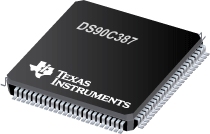
DS90C387 - +3.3V 双像素 LVDS 显示接口 (LDI)-SVGA/QXGA
DS90C387是TI德州仪器公司的一款FlatLink/FPD-Link(用于LCD的LVDS)产品,DS90C387是+3.3V 双像素 LVDS 显示接口 (LDI)-SVGA/QXGA,本站介绍了DS90C387的封装应用图解、特点和优点、功能等,并给出了与DS90C387相关的TI元器件型号供参考。
DS90C387 - +3.3V 双像素 LVDS 显示接口 (LDI)-SVGA/QXGA - FlatLink/FPD-Link(用于LCD的LVDS) - 显示和成像串行器/解串器 - 德州仪器
The DS90C387/DS90CF388 transmitter/receiver pair is designed to support dual pixel data transmission between Host and Flat Panel Display up to QXGA resolutions. The transmitter converts 48 bits (Dual Pixel 24-bit color) of CMOS/TTL data into 8 LVDS (Low Voltage Differential Signalling) data streams. Control signals (VSYNC, HSYNC, DE and two user-defined signals) are sent during blanking intervals. At a maximum dual pixel rate of 112MHz, LVDS data line speed is 672Mbps, providing a total throughput of 5.38Gbps (672 Megabytes per second). Two other modes are also supported. 24-bit color data (single pixel) can be clocked into the transmitter at a maximum rate of 170MHz. In this mode, the transmitter provides single-to-dual pixel conversion, and the output LVDS clock rate is 85MHz maximum. The third mode provides inter-operability with FPD-Link devices.
The LDI chipset is improved over prior generations of FPD-Link devices and offers higher bandwidth support and longer cable drive with three areas of enhancement. To increase bandwidth, the maximum pixel clock rate is increased to 112 (170) MHz and 8 serialized LVDS outputs are provided. Cable drive is enhanced with a user selectable pre-emphasis feature that provides additional output current during transitions to counteract cable loading effects. DC balancing on a cycle-to-cycle basis, is also provided to reduce ISI (Inter-Symbol Interference). With pre-emphasis and DC balancing, a low distortion eye-pattern is provided at the receiver end of the cable. A cable deskew capability has been added to deskew long cables of pair-to-pair skew of up to +/−1 LVDS data bit time (up to 80 MHz Clock Rate). These three enhancements allow cables 5+ meters in length to be driven. This chipset is an ideal means to solve EMI and cable size problems for high-resolution flat panel applications. It provides a reliable interface based on LVDS technology that delivers the bandwidth needed for high-resolution panels while maximizing bit times, and keeping clock rates low to reduce EMI and shielding requirements. For more details, please refer to .
- Complies with OpenLDI Specification for Digital Display Interfaces
- 32.5 to 112/170MHz Clock Support for DS90C387, 40 to 112MHz Clock Support for DS90CF388
- Supports SVGA through QXGA Panel Resolutions
- Drives Long, Low Cost Cables
- Up to 5.38Gbps Bandwidth
- Pre-Emphasis Reduces Cable Loading Effects
- DC Balance Data Transmission Provided by Transmitter Reduces ISI Distortion
- Cable Deskew of +/−1 LVDS Data Bit Time (up to 80 MHz Clock Rate) of Pair-to-Pair Skew at Receiver Inputs; Intra-Pair Skew Tolerance of 300ps
- Dual Pixel Architecture Supports Interface to GUI and Timing Controller; Optional Single Pixel Transmitter Inputs Support Single Pixel GUI Interface
- Transmitter Rejects Cycle-to-Cycle Jitter
- 5V Tolerant on Data and Control Input Pins
- Programmable Transmitter Data and Control Strobe Select (Rising or Falling Edge Strobe)
- Backward Compatible Configuration Select with FPD-Link
- Optional Second LVDS Clock for Backward Compatibility w/ FPD-Link
- Support for Two Additional User-Defined Control Signals in DC Balanced Mode
- Compatible with ANSI/TIA/EIA-644-1995 LVDS Standard
- DAC7716 - 四路 12 位高准确度 +/-16.5V 输出串行输入数模转换器
- SN65LBC176A-EP - 增强型产品差动总线收发器
- ADS5240 - 具有串行 LVDS 接口的 4 通道 12 位 40MSPS ADC
- TPS77625-EP - 增强型产品快速瞬态响应 500Ma 低压降稳压器
- LM3561 - Synchronous Boost Converter with 600mA High Side LED Driver and I2C-Compatible Interface
- TLV320ADC3001 - 92dB SNR 低功耗立体声 ADC (ADC3001)
- TPS82677 - 600mA、高效 MicroSiP? 降压转换器模块(厚度 <1.0mm)。
- TPS54519 - 2.95V 至 6V 输入、5A 同步降压 SWIFT? 转换器
- TL750M05 - 单输出 LDO、750mA、固定电压 (5.0V)、低静态电流、60V 负载突降保护
- INA168-Q1 - 汽车级、60V、高侧、电流输出电流分流监控器

