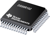

DS99R102是TI公司的一款FPD-LinkII串行器/解串器产品,DS99R102是3-40MHz DC 平衡 24 位 LVDS 解串器,本页介绍了DS99R102的产品说明、应用、特性等,并给出了与DS99R102相关的TI元器件型号供参考。
DS99R102 - 3-40MHz DC 平衡 24 位 LVDS 解串器 - FPD-LinkII串行器/解串器 - 显示和成像串行器/解串器 - TI公司(Texas Instruments,德州仪器)
The DS99R101/DS99R102 Chipset translates a 24-bit parallel bus into a fully transparent data/control LVDS serial stream with embedded clock information. This single serial stream simplifies transferring a 24-bit bus over PCB traces and cable by eliminating the skew problems between parallel data and clock paths. It saves system cost by narrowing data paths that in turn reduce PCB layers, cable width, and connector size and pins.
The DS99R101/DS99R102 incorporates LVDS signaling on the high-speed I/O. LVDS provides a low power and low noise environment for reliably transferring data over a serial transmission path. By optimizing the serializer output edge rate for the operating frequency range EMI is further reduced.
Internal DC balanced encoding/decoding is used to support AC-Coupled interconnects.
- 3 MHz–40 MHz Clock Embedded and DC-Balancing 24:1 and 1:24 Data Transmissions
- User Selectable Clock Edge for Parallel Data on Both Transmitter and Receiver
- Internal DC Balancing Encode/Decode – Supports AC-Coupling Interface with No External Coding Required
- Individual Power-Down Controls for Both Transmitter and Receiver
- Embedded Clock CDR (Clock and Data Recovery) on Receiver and No External Source of Reference Clock Needed
- All Codes RDL (Random Data Lock) to Support Live-Pluggable Applications
- LOCK Output Flag to Ensure Data Integrity at Receiver Side
- Balanced TSETUP/THOLD Between RCLK and RDATA on Receiver Side
- PTO (Progressive Turn-On) LVCMOS Outputs to Reduce EMI and Minimize SSO Effects
- All LVCMOS Inputs and Control Pins Have Internal Pulldown
- On-Chip Filters for PLLs on Transmitter and Receiver
- 48-Pin TQFP Package
- Pure CMOS .35 μm Process
- Power Supply Range 3.3V ± 10%
- Temperature Range 0°C to +70°C
- 8 kV HBM ESD Tolerance


