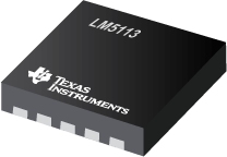

LM5113是TI公司的一款GaNFET驱动器产品,LM5113是增强模式 GaN FET 的 5A、100V 半桥接闸极驱动器,本页介绍了LM5113的产品说明、应用、特性等,并给出了与LM5113相关的TI元器件型号供参考。
LM5113 - 增强模式 GaN FET 的 5A、100V 半桥接闸极驱动器 - GaNFET驱动器 - 氮化镓(GaN)?解决方案 - TI公司(Texas Instruments,德州仪器)
The LM5113 is designed to drive both the high-side and the low-side enhancement mode Gallium Nitride (GaN) FETs in a synchronous buck or a half bridge configuration. The floating high-side driver is capable of driving a high-side enhancement mode GaN FET operating up to 100V. The high-side bias voltage is generated using a bootstrap technique and is internally clamped at 5.2V, which prevents the gate voltage from exceeding the maximum gate-source voltage rating of enhancement mode GaN FETs. The inputs of the LM5113 are TTL logic compatible, and can withstand input voltages up to 14V regardless of the VDD voltage. The LM5113 has split gate outputs, providing flexibility to adjust the turn-on and turn-off strength independently.
In addition, the strong sink capability of the LM5113 maintains the gate in the low state, preventing unintended turn-on during switching. The LM5113 can operate up to several MHz. The LM5113 is available in a standard WSON-10 pin package and a 12-bump DSBGA package. The WSON-10 pin package contains an exposed pad to aid power dissipation. The DSBGA package offers a compact footprint and minimized package inductance.
- Independent High-Side and Low-Side TTL Logic Inputs
- 1.2A/5A Peak Source/Sink Current
- High-Side Floating Bias Voltage Rail Operates up to 100VDC
- Internal Bootstrap Supply Voltage Clamping
- Split Outputs for Adjustable Turn-on/Turn-off Strength
- 0.6? /2.1? Pull-down/Pull-up Resistance
- Fast Propagation Times (28ns Typical)
- Excellent Propagation Delay Matching (1.5ns Typical)
- Supply Rail Under-Voltage Lockout
- Low Power Consumption
- Packages
- WSON-10 (4 mm x 4 mm)
- DSBGA (2 mm x 2 mm)


