


- MSP430FR2032IG48 - МЏГЩЕчТЗЃЈICЃЉ > ЧЖШыЪН > ЮЂПижЦЦї
- TMCS1101A1BQDRQ1 - ДЋИаЦїЃЌБфЫЭЦї > ЕчСїДЋИаЦї
- MSP430F2419TZQW - МЏГЩЕчТЗЃЈICЃЉ > ЧЖШыЪН > ЮЂПижЦЦї
- TPS62042DRCR - МЏГЩЕчТЗЃЈICЃЉ > ЕчдДЙмРэЃЈPMICЃЉ > ЮШбЙЦї - DC-DC ПЊЙиЮШбЙЦї
- SN75ALS171J - МЏГЩЕчТЗЃЈICЃЉ > НгПк > Ч§ЖЏЦїЃЌНгЪеЦїЃЌЪеЗЂЦї
- 2510442-0005 - МЏГЩЕчТЗЃЈICЃЉ > зЈгУ IC
- LM5034MTC - МЏГЩЕчТЗЃЈICЃЉ > ЕчдДЙмРэЃЈPMICЃЉ > DC-DC ПЊЙиПижЦЦї
- LM706A0QEVM - ПЊЗЂАхЃЌЬзМўЃЌБрГЬЦї > ЦРЙРАх > DC/DC КЭ AC/DCЃЈРыЯпЃЉSMPS ЦРЙРАх
- LM4549BVHX - МЏГЩЕчТЗЃЈICЃЉ > НгПк > БрНтТыЦї
- SN74LVTH541NS - МЏГЩЕчТЗЃЈICЃЉ > ТпМ > ЛКГхЦїЃЌЧ§ЖЏЦїЃЌНгЪеЦїЃЌЪеЗЂЦї
- SD044EVK - ЦРЙРКЭбнЪОАхМАЬзМў
- SN74LVC1G14DCKTG4 - МЏГЩЕчТЗЃЈICЃЉ > ТпМ > УХКЭЗДЯрЦї
- TUSB1004IRNQR - МЏГЩЕчТЗЃЈICЃЉ > НгПк > аХКХЛКГхЦїЁЂжаМЬЦїЁЂЗжРыЦї
- LM3880QMFE-1AA/NOPB - МЏГЩЕчТЗЃЈICЃЉ > ЕчдДЙмРэЃЈPMICЃЉ > ЕчдДПижЦЦїЃЌМрЪгЦї
- LM318DRG4 - МЏГЩЕчТЗЃЈICЃЉ > Япад > ЗХДѓЦї > вЧЦїЃЌдЫЫуЗХДѓЦїЃЌЛКГхЦї
- TPS65052RSMT - МЏГЩЕчТЗЃЈICЃЉ > ЕчдДЙмРэЃЈPMICЃЉ > ЕчдДЙмРэ - зЈгУ
- TPS62260DDCT - МЏГЩЕчТЗЃЈICЃЉ > ЕчдДЙмРэЃЈPMICЃЉ > ЮШбЙЦї - DC-DC ПЊЙиЮШбЙЦї
- LM4132BMF-2.0/NOPB - МЏГЩЕчТЗЃЈICЃЉ > ЕчдДЙмРэЃЈPMICЃЉ > ЕчбЙЛљзМ
- TPS92623Q1EVM - ПЊЗЂАхЃЌЬзМўЃЌБрГЬЦї > ЦРЙРАх > LED Ч§ЖЏЦїЦРЙРАх
- BQ24075RGTR - МЏГЩЕчТЗЃЈICЃЉ > ЕчдДЙмРэЃЈPMICЃЉ > ЕчГиГфЕчЦї


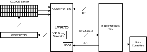
LM98725 - Опга LVDS/CMOS ЪфГіКЭМЏГЩ CCD/CIS ДЋИаЦїЖЈЪБЗЂЫЭЦїЕФ 3 ЭЈЕР 16 ЮЛ 81 MSPS AFE
LM98725ЪЧTIЕТжнвЧЦїЙЋЫОЕФвЛПюCCD/CMOSаХКХЕїНкВњЦЗЃЌLM98725ЪЧОпга LVDS/CMOS ЪфГіКЭМЏГЩ CCD/CIS ДЋИаЦїЖЈЪБЗЂЫЭЦїЕФ 3 ЭЈЕР 16 ЮЛ 81 MSPS AFEЃЌБОеОНщЩмСЫLM98725ЕФЗтзАгІгУЭМНтЁЂЬиЕуКЭгХЕуЁЂЙІФмЕШЃЌВЂИјГіСЫгыLM98725ЯрЙиЕФTIдЊЦїМўаЭКХЙЉВЮПМЁЃ
LM98725 - Опга LVDS/CMOS ЪфГіКЭМЏГЩ CCD/CIS ДЋИаЦїЖЈЪБЗЂЫЭЦїЕФ 3 ЭЈЕР 16 ЮЛ 81 MSPS AFE - CCD/CMOSаХКХЕїНк - ФЃФтЧАЖЫ(AFE) - ЕТжнвЧЦї
- LVDS/CMOS Outputs
- LVDS/CMOS/Crystal Clock Source with PLL Multiplication
- Integrated Flexible Spread Spectrum Clock Generation
- CDS or S/H Processing for CCD or CIS Sensors
- Independent Gain/Offset Correction for Each Channel
- Automatic per-Channel Gain and Offset Calibration
- Programmable Input Clamp Voltage
- Flexible CCD/CIS Sensor Timing Generator
- Multi-Function Peripherals
- High-speed Currency/Check Scanners
- Flatbed or Handheld Color Scanners
- High-speed Document Scanners
- Key Specifications:
- Maximum Input Level
- 1.2 or 2.4 Volt Modes
- (Both with + or - Polarity Option)
- ADC Resolution: 16-Bit
- ADC Sampling Rate: 81 MSPS
- INL: +17/- 28 LSB (typ)
- Channel Sampling Rate: 30/30/27 MSPS
- PGA Gain Steps: 256 Steps
- PGA Gain Range: 0.62 to 8.3x
- Analog DAC Resolution: ±9 Bits
- Analog DAC Range: ±307 mV or ±614 mV
- Digital DAC Resolution: ±6 Bits
- Digital DAC Range: -2048 LSB to + 2016 LSB
- SNR: –74dB (@0 dB PGA Gain)
- Power Dissipation: 755 mW (LVDS)
- Operating Temp: 0 to 70°C
- Supply Voltage: 3.3 V Nominal (3.0-V to 3.6-V Range)
- Maximum Input Level
The LM98725 is a fully integrated, high performance 16-Bit, 81 MSPS signal processing solution for digital color copiers, scanners, and other image processing applications. The LM98725 achieves high-speed signal throughput with an innovative architecture utilizing Correlated Double Sampling (CDS), typically employed with CCD arrays, or Sample and Hold (S/H) inputs (for higher speed CCD or CMOS image sensors). The signal paths utilize 8 bit Programmable Gain Amplifiers (PGA), a ±9-Bit offset correction DAC, and independently controlled Digital Black Level correction loops for each input. The independently programmed PGA and offset DAC allow unique values of gain and offset for each of the three analog inputs. The signals are then routed to a 81 MHz high performance analog-to-digital converter (ADC). The fully differential processing channel shows exceptional noise immunity with a very low noise floor of –74 dB. The 16-bit ADC has excellent dynamic performance making the LM98725 transparent in the image reproduction chain.
A very flexible integrated Spread Spectrum Clock Generation (SSCG) modulator is included to assist with EM compliance and reduce system costs.
| PART NUMBER | PACKAGE | BODY SIZE (NOM) |
|---|---|---|
| LM98725 | TSSOP (56) | 14.0 mm × 6.10 mm |
- DS90CP22 - 800 Mbps 2x2 LVDS НЛВцЕуНЛЛЛЦї
- TPS51225 - Dual Synchronous Step-Down Controller with 5-V and 3.3-V LDOs
- ADS7951 - 12 ЮЛЁЂ1 MSPSЁЂ8 ЭЈЕРЁЂЕЅЖЫЁЂSAR ADC
- CD54HCT158 - ИпЫй CMOS ТпМЫФТЗ 2 ЪфШыЖрТЗИДгУЦї
- CD74HCT132 - ИпЫй CMOS ТпМЫФТЗЪЉУмЬиДЅЗЂ 2 ЪфШыгыЗЧУХ
- DP83843 - PHYTER
- LP38512-ADJ - 1.5A Fast-Transient Response Adjustable Low-Dropout Linear Voltage Regulator
- LP2980-N - ВЩгУ SOT-23 ЗтзАЕФЮЂЙІКФ 50 mA ГЌЕЭбЙНЕЮШбЙЦї
- ADS7835 - 12 ЮЛИпЫйЕЭЙІКФВЩбљФЃЪ§зЊЛЛЦї
- DS92LV2422 - 10 жС 75 MHzЃЌ24 ЮЛЦЕЕРСДНг II НтДЎЦї

