


- SN74AC08MDREP - 集成电路(IC) > 逻辑 > 门和反相器
- TLV379IDR - 集成电路(IC) > 线性 > 放大器 > 仪器,运算放大器,缓冲器
- SN74AHC74PW - 集成电路(IC) > 逻辑 > 触发器
- TLV2632ID - 集成电路(IC) > 线性 > 放大器 > 仪器,运算放大器,缓冲器
- LM96194CISQ/NOPB - 集成电路(IC) > 电源管理(PMIC) > 热管理
- TAS5424TDKDQ1 - 集成电路(IC) > 线性 > 放大器 > 音频放大器
- TPS92515HVEVM-749 - 开发板,套件,编程器 > 评估板 > LED 驱动器评估板
- SN74AS652FN - 集成电路(IC) > 逻辑 > 缓冲器,驱动器,接收器,收发器
- TPS53310RGTT - 集成电路(IC) > 电源管理(PMIC) > 稳压器 - DC-DC 开关稳压器
- TPS22922BEVM - 开发板,套件,编程器 > 评估板 > 评估和演示板及套件
- TPS73201DRBT - 集成电路(IC) > 电源管理(PMIC) > 稳压器 - 线性
- TSW3082EVM - 开发板,套件,编程器 > 评估板 > 数模转换器(DAC)评估板
- DAC7724UB - 集成电路(IC) > 数据采集 > 数模转换器(DAC)
- SN74ALS653DWE4 - 集成电路(IC) > 逻辑 > 缓冲器,驱动器,接收器,收发器
- BQ296222DSGR - 集成电路(IC) > 电源管理(PMIC) > 电池管理
- TPIC44L02DBG4 - 集成电路(IC) > 电源管理(PMIC) > 栅极驱动器
- TMDSEVM6424 - 开发板,套件,编程器 > 评估板 > 嵌入式 MCU、DSP 评估板
- LMK04805BISQX/NOPB - 集成电路(IC) > 时钟/定时 > 时钟发生器,PLL,频率合成器
- LP3470IM5X-4.38 - 集成电路(IC) > 电源管理(PMIC) > 监控器
- ISOM8111DFGRQ1 - 隔离器 > 光隔离器 > 晶体管,光电输出光隔离器


OMAP-L132 - OMAP-L132 C6-Integra DSP+ARM Processor
OMAP-L132是TI德州仪器公司的一款C6000DSP+ARM处理器产品,OMAP-L132是OMAP-L132 C6-Integra DSP+ARM Processor,本站介绍了OMAP-L132的封装应用图解、特点和优点、功能等,并给出了与OMAP-L132相关的TI元器件型号供参考。
OMAP-L132 - OMAP-L132 C6-Integra DSP+ARM Processor - C6000DSP+ARM处理器 - 数字信号处理器 - 德州仪器
- Dual-Core SoC
- 200-MHz ARM926EJ-S™ RISC MPU
- 200-MHz C674x Fixed- and Floating-Point VLIW DSP
- ARM926EJ-S Core
- 32- and 16-Bit (Thumb®) Instructions
- DSP Instruction Extensions
- Single-Cycle MAC
- ARM Jazelle® Technology
- Embedded ICE-RT™ for Real-Time Debug
- ARM9™ Memory Architecture
- 16KB of Instruction Cache
- 16KB of Data Cache
- 8KB of RAM (Vector Table)
- 64KB of ROM
- C674x Instruction Set Features
- Superset of the C67x+ and C64x+ ISAs
- Up to 1600 MIPS and 1200 MFLOPS
- Byte-Addressable (8-, 16-, 32-, and 64-Bit Data)
- 8-Bit Overflow Protection
- Bit-Field Extract, Set, Clear
- Normalization, Saturation, Bit-Counting
- Compact 16-Bit Instructions
- C674x Two-Level Cache Memory Architecture
- 32KB of L1P Program RAM/Cache
- 32KB of L1D Data RAM/Cache
- 256KB of L2 Unified Mapped RAM/Cache
- Flexible RAM/Cache Partition (L1 and L2)
- Enhanced Direct Memory Access Controller 3 (EDMA3):
- 2 Channel Controllers
- 3 Transfer Controllers
- 64 Independent DMA Channels
- 16 Quick DMA Channels
- Programmable Transfer Burst Size
- TMS320C674x Floating-Point VLIW DSP Core
- Load-Store Architecture with Nonaligned Support
- 64 General-Purpose Registers (32-Bit)
- Six ALU (32- and 40-Bit) Functional Units
- Supports 32-Bit Integer, SP (IEEE Single Precision/32-Bit) and DP (IEEE Double Precision/64-Bit) Floating Point
- Supports up to Four SP Additions Per Clock, Four DP Additions Every Two Clocks
- Supports up to Two Floating-Point (SP or DP) Reciprocal Approximation (RCPxP) and Square-Root Reciprocal Approximation (RSQRxP) Operations Per Cycle
- Two Multiply Functional Units:
- Mixed-Precision IEEE Floating-Point Multiply Supported up to:
- 2 SP x SP → SP Per Clock
- 2 SP x SP → DP Every Two Clocks
- 2 SP x DP → DP Every Three Clocks
- 2 DP x DP → DP Every Four Clocks
- Fixed-Point Multiply Supports Two 32 x 32-Bit Multiplies, Four 16 x 16-Bit Multiplies, or Eight 8 x 8-Bit Multiplies per Clock Cycle, and Complex Multiples
- Mixed-Precision IEEE Floating-Point Multiply Supported up to:
- Instruction Packing Reduces Code Size
- All Instructions Conditional
- Hardware Support for Modulo Loop Operation
- Protected Mode Operation
- Exceptions Support for Error Detection and Program Redirection
- Software Support
- TI DSPBIOS™
- Chip Support Library and DSP Library
- 128KB of RAM Shared Memory
- 1.8-V or 3.3-V LVCMOS I/Os (Except for USB and DDR2 Interfaces)
- Two External Memory Interfaces:
- EMIFA
- NOR (8- or 16-Bit-Wide Data)
- NAND (8- or 16-Bit-Wide Data)
- 16-Bit SDRAM with 128-MB Address Space
- DDR2/Mobile DDR Memory Controller with one of the following:
- 16-Bit DDR2 SDRAM with 256-MB Address Space
- 16-Bit mDDR SDRAM with 256-MB Address Space
- Three Configurable 16550-Type UART Modules:
- With Modem Control Signals
- 16-Byte FIFO
- 16x or 13x Oversampling Option
- Two Serial Peripheral Interfaces (SPIs) Each with Multiple Chip Selects
- Two Multimedia Card (MMC)/Secure Digital (SD) Card Interfaces with Secure Data I/O (SDIO) Interfaces
- Two Master and Slave Inter-Integrated Circuits (I2C Bus™)
- Programmable Real-Time Unit Subsystem (PRUSS)
- Two Independent Programmable Real-Time Unit (PRU) Cores
- 32-Bit Load-Store RISC Architecture
- 4KB of Instruction RAM Per Core
- 512 Bytes of Data RAM Per Core
- PRUSS can be Disabled via Software to Save Power
- Register 30 of Each PRU is Exported From the Subsystem in Addition to the Normal R31 Output of the PRU Cores.
- Standard Power-Management Mechanism
- Clock Gating
- Entire Subsystem Under a Single PSC Clock Gating Domain
- Dedicated Interrupt Controller
- Dedicated Switched Central Resource
- USB 2.0 OTG Port with Integrated PHY (USB0)
- USB 2.0 High- and Full-Speed Client
- USB 2.0 High-, Full-, and Low-Speed Host
- End Point 0 (Control)
- End Points 1,2,3,4 (Control, Bulk, Interrupt, or ISOC) RX and TX
- One Multichannel Audio Serial Port (McASP):
- Two Clock Zones and 16 Serial Data Pins
- Supports TDM, I2S, and Similar Formats
- DIT-Capable
- FIFO Buffers for Transmit and Receive
- Two Multichannel Buffered Serial Ports (McBSPs):
- Supports TDM, I2S, and Similar Formats
- AC97 Audio Codec Interface
- Telecom Interfaces (ST-Bus, H100)
- 128-Channel TDM
- FIFO Buffers for Transmit and Receive
- 10/100 Mbps Ethernet MAC (EMAC):
- IEEE 802.3 Compliant
- MII Media-Independent Interface
- RMII Reduced Media-Independent Interface
- Management Data I/O (MDIO) Module
- Real-Time Clock (RTC) with 32-kHz Oscillator and Separate Power Rail
- Three 64-Bit General-Purpose Timers (Each Configurable as Two 32-Bit Timers)
- One 64-Bit General-Purpose or Watchdog Timer (Configurable as Two 32-Bit General-Purpose Timers)
- Two Enhanced High-Resolution Pulse Width Modulators (eHRPWMs):
- Dedicated 16-Bit Time-Base Counter with Period and Frequency Control
- 6 Single-Edge Outputs, 6 Dual-Edge Symmetric Outputs, or 3 Dual-Edge Asymmetric Outputs
- Dead-Band Generation
- PWM Chopping by High-Frequency Carrier
- Trip Zone Input
- Three 32-Bit Enhanced Capture (eCAP) Modules:
- Configurable as 3 Capture Inputs or 3 Auxiliary Pulse Width Modulator (APWM) Outputs
- Single-Shot Capture of up to Four Event Time-Stamps
- Packages:
- 361-Ball Pb-Free PBGA [ZWT Suffix], 0.80-mm Ball Pitch
- Commercial or Extended Temperature
- Professional or Private Mobile Radio (PMR)
- Industrial Automation
- Biometric Identification
- Smart Grid Substation Protection
- Industrial Portable Navigation Devices
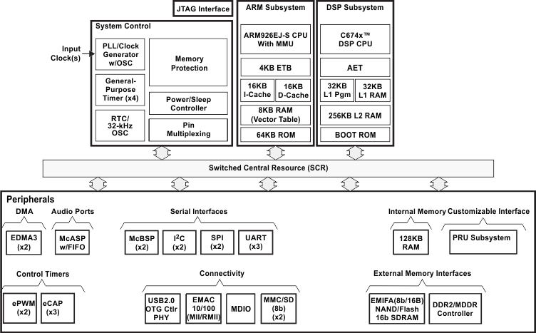
The OMAP-L132 C6000 DSP+ARM processor is a low-power applications processor based on an ARM926EJ-S and a C674x DSP core. This processor provides significantly lower power than other members of the TMS320C6000™ platform of DSPs.
The device enables original-equipment manufacturers (OEMs) and original-design manufacturers (ODMs) to quickly bring to market devices with robust operating systems, rich user interfaces, and high processor performance through the maximum flexibility of a fully integrated, mixed processor solution.
The dual-core architecture of the device provides benefits of both DSP and reduced instruction set computer (RISC) technologies, incorporating a high-performance TMS320C674x DSP core and an ARM926EJ-S core.
The ARM926EJ-S is a 32-bit RISC processor core that performs 32-bit or 16-bit instructions and processes 32-bit, 16-bit, or 8-bit data. The core uses pipelining so that all parts of the processor and memory system can operate continuously.
The ARM9 core has a coprocessor 15 (CP15), protection module, and data and program memory management units (MMUs) with table look-aside buffers. The ARM9 core has separate 16-KB instruction and 16-KB data caches. Both are 4-way associative with virtual index virtual tag (VIVT). The ARM9 core also has 8KB of RAM (Vector Table) and 64KB of ROM.
The device DSP core uses a 2-level cache-based architecture. The level 1 program cache (L1P) is a 32-KB direct mapped cache, and the level 1 data cache (L1D) is a 32-KB 2-way, set-associative cache. The level 2 program cache (L2P) consists of a 256-KB memory space that is shared between program and data space. L2 memory can be configured as mapped memory, cache, or combinations of the two. Although the DSP L2 is accessible by the ARM9 and other hosts in the system, an additional 128KB of RAM shared memory is available for use by other hosts without affecting DSP performance.
For security-enabled devices, TI’s Basic Secure Boot lets users protect proprietary intellectual property and prevents external entities from modifying user-developed algorithms. By starting from a hardware-based “root-of-trust”, the secure boot flow ensures a known good starting point for code execution. By default, the JTAG port is locked down to prevent emulation and debug attacks; however, the JTAG port can be enabled during the secure boot process during application development. The boot modules are encrypted while sitting in external nonvolatile memory, such as flash or EEPROM, and are decrypted and authenticated when loaded during secure boot. Encryption and decryption protects customers’ IP and lets them securely set up the system and begin device operation with known, trusted code.
Basic Secure Boot uses either SHA-1 or SHA-256, and AES-128 for boot image validation. Basic Secure Boot also uses AES-128 for boot image encryption. The secure boot flow employs a multilayer encryption scheme which not only protects the boot process but offers the ability to securely upgrade boot and application software code. A 128-bit device-specific cipher key, known only to the device and generated using a NIST-800-22 certified random number generator, is used to protect customer encryption keys. When an update is needed, the customer creates a new encrypted image. Then the device can acquire the image through an external interface, such as Ethernet, and overwrite the existing code. For more details on the supported security features or TI’s Basic Secure Boot, refer to the TMS320C674x/OMAP-L1x Processor Security User’s Guide (SPRUGQ9).
The peripheral set includes: a 10/100 Mbps Ethernet media access controller (EMAC) with a management data input/output (MDIO) module; one USB2.0 OTG interface; two I2C Bus interfaces; one multichannel audio serial port (McASP) with 16 serializers and FIFO buffers; two multichannel buffered serial ports (McBSPs) with FIFO buffers; two serial peripheral interfaces (SPIs) with multiple chip selects; four 64-bit general-purpose timers each configurable (one configurable as a watchdog); a configurable 16-bit host-port interface (HPI); up to 9 banks of general-purpose input/output (GPIO) pins, with each bank containing 16 pins with programmable interrupt and event generation modes, multiplexed with other peripherals; three UART interfaces (each with RTS and CTS); two enhanced high-resolution pulse width modulator (eHRPWM) peripherals; three 32-bit enhanced capture (eCAP) module peripherals which can be configured as 3 capture inputs or 3 APWM outputs; two external memory interfaces: an asynchronous and SDRAM external memory interface (EMIFA) for slower memories or peripherals; and a higher speed DDR2/Mobile DDR controller.
The EMAC provides an efficient interface between the device and a network. The EMAC supports both 10Base-T and 100Base-TX, or 10 Mbps and 100 Mbps in either half- or full-duplex mode. Additionally, an MDIO interface is available for PHY configuration. The EMAC supports both MII and RMII interfaces.
The rich peripheral set provides the ability to control external peripheral devices and communicate with external processors. For details on each of the peripherals, see the related sections in this document and the associated peripheral reference guides.
The device has a complete set of development tools for the ARM9 and DSP. These tools include C compilers, a DSP assembly optimizer to simplify programming and scheduling, and a Windows® debugger interface for visibility into source code execution.
| PART NUMBER | PACKAGE | BODY SIZE |
|---|---|---|
| OMAPL132ZWT | NFBGA (361) | 16,00 mm x 16,00 mm |
- TPS3824-25-Q1 - 具有看门狗输入、RESET 和 /RESET 的汽车类电源电压监控器
- CD54HC574 - 具有三态输出的高速 CMOS 逻辑八路上升沿 D 类触发器
- LM60-Q1 - 汽车用 2.7V、SOT-23 或 TO-92 温度传感器
- CDCV850 - 2.5V 锁相环差动时钟驱动器,具有 2 线路串行接口
- CSD17570Q5B - 30V,N 通道 NexFET 功率 MOSFET,CSD17570Q5B
- TPS2051B - 单路限流配电开关
- MSP430G2232 - MSP430G2x32、MSP430G2x02 混合信号微处理器
- SN54AHC00 - 四路 2 输入正与非门
- MSP430F5255 - MSP430F5259 混合信号微控制器
- TPS2148 - 用于 USB 外设的 3.3V LDO + 双路开关,工作态低电平启用

