


- HPA02230AIDBVR - 电源管理IC - 电流调节和管理
- INA310A5QDGKRQ1 - 集成电路(IC) > 线性 > 放大器 > 仪器,运算放大器,缓冲器
- CY74FCT2574TSOCT - 集成电路(IC) > 逻辑 > 触发器
- SN65LVDS1DG4 - 集成电路(IC) > 接口 > 驱动器,接收器,收发器
- SN74AUP1G07DSF2 - 集成电路(IC) > 逻辑 > 缓冲器,驱动器,接收器,收发器
- LP2951ACMMX-3.0/NOPB - 集成电路(IC) > 电源管理(PMIC) > 稳压器 - 线性
- TL432ACDBZR - 集成电路(IC) > 电源管理(PMIC) > 电压基准
- ADS127L11IPWR - 集成电路(IC) > 数据采集 > 模数转换器(ADC)
- SN74LV165ADRE4 - 集成电路(IC) > 逻辑 > 移位寄存器
- LM306D - 集成电路(IC) > 线性 > 比较器
- PTH04T260WAST - 板安装电源 > 直流转换器
- SN74AS34N - 集成电路(IC) > 逻辑 > 缓冲器,驱动器,接收器,收发器
- SN75HVD07P - 集成电路(IC) > 接口 > 驱动器,接收器,收发器
- INA241A1QDGSRQ1 - 集成电路(IC) > 线性 > 放大器 > 仪器,运算放大器,缓冲器
- UCC28600EVM-65W - 开发板,套件,编程器 > 评估板 > DC/DC 和 AC/DC(离线)SMPS 评估板
- SN74AUC1G08YZAR - 集成电路(IC) > 逻辑 > 门和反相器
- TPA3000D1PWP - 集成电路(IC) > 线性 > 放大器 > 音频放大器
- OPA37GP - 集成电路(IC) > 线性 > 放大器 > 仪器,运算放大器,缓冲器
- SNJ54HC21FK - 集成电路(IC) > 逻辑 > 门和反相器
- TPS79318YEQEVM - 开发板,套件,编程器 > 评估板 > 线性稳压器评估板


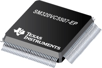
SM320VC5507-EP - 增强型产品定点数字信号处理器
SM320VC5507-EP是TI德州仪器公司的一款C5000DSP产品,SM320VC5507-EP是增强型产品定点数字信号处理器,本站介绍了SM320VC5507-EP的封装应用图解、特点和优点、功能等,并给出了与SM320VC5507-EP相关的TI元器件型号供参考。
SM320VC5507-EP - 增强型产品定点数字信号处理器 - C5000DSP - 数字信号处理器 - 德州仪器
The SM320VC5507 fixed-point digital signal processor (DSP) is based on the SMS320C55x DSP generation CPU processor core. The C55x™ DSP architecture achieves high performance and low power through increased parallelism and total focus on reduction in power dissipation. The CPU supports an internal bus structure that is composed of one program bus, three data read buses, two data write buses, and additional buses dedicated to peripheral and DMA activity. These buses provide the ability to perform up to three data reads and two data writes in a single cycle. In parallel, the DMA controller can perform up to two data transfers per cycle independent of the CPU activity.
The C55x CPU provides two multiply-accumulate (MAC) units, each capable of 17-bit x 17-bit multiplication in a single cycle. A central 40-bit arithmetic/logic unit (ALU) is supported by an additional 16-bit ALU. Use of the ALUs is under instruction set control, providing the ability to optimize parallel activity and power consumption. These resources are managed in the Address Unit (AU) and Data Unit (DU) of the C55x CPU.
The C55x DSP generation supports a variable byte width instruction set for improved code density. The Instruction Unit (IU) performs 32-bit program fetches from internal or external memory and queues instructions for the Program Unit (PU). The Program Unit decodes the instructions, directs tasks to AU and DU resources, and manages the fully protected pipeline. Predictive branching capability avoids pipeline flushes on execution of conditional instructions.
The 128K bytes of on-chip memory on 5507 is sufficient for many hand-held appliances, portable GPS systems, wireless speaker phones, portable PDAs, and gaming devices. Many of these appliances typically require 64K bytes or more on-chip memory but less than 128K bytes of memory, and need to operate in standby mode for more than 60% to 70% of time. For the applications which require more than 128K bytes of on-chip memory but less than 256K bytes of on-chip memory, Texas Instruments (TI) offers the TMS320VC5509A device, which is based on the TMS320C55x DSP core.
The general-purpose input and output functions and the10-bit A/D provide sufficient pins for status, interrupts, and bit I/O for LCDs, keyboards, and media interfaces. The parallel interface operates in two modes, either as a slave to a microcontroller using the HPI port or as a parallel media interface using the asynchronous EMIF. Serial media is supported through three McBSPs.
The 5507 peripheral set includes an external memory interface (EMIF) that provides glueless access to asynchronous memories like EPROM and SRAM, as well as to high-speed, high-density memories such as synchronous DRAM. Additional peripherals include Universal Serial Bus (USB), real-time clock, watchdog timer, and I2C multi-master and slave interface. Three full-duplex multichannel buffered serial ports (McBSPs) provide glueless interface to a variety of industry-standard serial devices, and multichannel communication with up to 128 separately enabled channels. The enhanced host-port interface (HPI) is a 16-bit parallel interface used to provide host processor access to 32K bytes of internal memory on the 5507. The HPI can be configured in either multiplexed or non-multiplexed mode to provide glueless interface to a wide variety of host processors. The DMA controller provides data movement for six independent channel contexts without CPU intervention, providing DMA throughput of up to two 16-bit words per cycle. Two general-purpose timers, up to eight dedicated general-purpose I/O (GPIO) pins, and digital phase-locked loop (DPLL) clock generation are also included.
The 5507 is supported by the industry’s award-winning eXpressDSP™, Code Composer Studio™ Integrated Development Environment (IDE), DSP/BIOS™, Texas Instruments’ algorithm standard, and the industry’s largest third-party network. The Code Composer Studio IDE features code generation tools including a C Compiler and Visual Linker, simulator, RTDX™, XDS510™ emulation device drivers, and evaluation modules. The 5507 is also supported by the C55x DSP Library which features more than 50 foundational software kernels (FIR filters, IIR filters, FFTs, and various math functions) as well as chip and board support libraries.
- High-Performance, Low-Power, Fixed-Point SMS320C5507 Digital Signal Processor
- 9.26-, 6.95-, 5-ns Instruction Cycle Time
- 108-, 144-, 200-MHz Clock Rate
- One/Two Instruction(s) Executed per Cycle
- Dual Multipliers (Up to 400 Million Multiply-Accumulates per Second (MMACS))
- Two Arithmetic/Logic Units (ALUs)
- Three Internal Data/Operand Read Buses and Two Internal Data/Operand Write Buses
- 64K x 16-Bit On-Chip RAM, Composed of:
- 64K Bytes of Dual-Access RAM (DARAM) 8 Blocks of 4K x 16-Bit
- 64K Bytes of Single-Access RAM (SARAM) 8 Blocks of 4K x 16-Bit
- 64K Bytes of One-Wait-State On-Chip ROM (32K x 16-Bit)
- 8M x 16-Bit Maximum Addressable External Memory Space (Synchronous DRAM)
- 16-Bit External Parallel Bus Memory Supporting Either:
- External Memory Interface (EMIF) With GPIO Capabilities and Glueless Interface to:
- Asynchronous Static RAM (SRAM)
- Asynchronous EPROM
- Synchronous DRAM (SDRAM)
- 16-Bit Parallel Enhanced Host-Port Interface (EHPI) With GPIO Capabilities
- External Memory Interface (EMIF) With GPIO Capabilities and Glueless Interface to:
- Programmable Low-Power Control of Six Device Functional Domains
- On-Chip Scan-Based Emulation Logic
- On-Chip Peripherals
- Two 20-Bit Timers
- Watchdog Timer
- Six-Channel Direct Memory Access (DMA) Controller
- Three Multichannel Buffered Serial Ports (McBSPs)
- Programmable Phase-Locked Loop Clock Generator
- Seven (LQFP) or Eight (BGA) General-Purpose I/O (GPIO) Pins and a General-Purpose Output Pin (XF)
- USB Full-Speed (12 Mbps) Slave Port Supporting Bulk, Interrupt and Isochronous Transfers
- Inter-Integrated Circuit (I2C) Multi-Master and Slave Interface
- Real-Time Clock (RTC) With Crystal Input, Separate Clock Domain, Separate Power Supply
- 4-Channel (BGA) or 2-Channel (LQFP) 10-Bit Successive Approximation A/D
- IEEE Std 1149.1(1) (JTAG) Boundary Scan Logic
- Packages:
- 144-Terminal Low-Profile Quad Flatpack (LQFP) (PGE Suffix)
- 1.2-V Core (108 MHz), 2.7-V – 3.6-V I/Os
- 1.35-V Core (144 MHz), 2.7-V – 3.6-V I/Os
- 1.6-V Core (200 MHz), 2.7-V – 3.6-V I/Os
- SUPPORTS DEFENSE, AEROSPACE, AND MEDICAL APPLICATIONS
- Controlled Baseline
- One Assembly/Test Site
- One Fabrication Site
- Available in Military (–55°C/125°C) Temperature Range(2)
- Extended Product Life Cycle
- Extended Product-Change Notification
- Product Traceability
(1) IEEE Standard 1149.1-1990 Standard-Test-Access Port and Boundary Scan Architecture. (2) Additional temperature ranges are available - contact factory C55x, eXpressDSP, Code Composer Studio, DSP/BIOS, RTDX, XDS510, TMS320, TMS320C5000, TMS320C55x, TMS320C55x are trademarks of Texas Instruments.
- SN74CBT16209A - 18 位 FET 总线交换开关
- SN5450 - 双路 2 宽度 2 输入与或反向门(一个门可扩展)
- CD54HCT10 - 高速 CMOS 逻辑三路 3 输入与非门
- TPD1E05U06 - 超低电容 ESD 保护设备系列
- ADC12C105 - 12 位、105 MSPS A/D 转换器
- SN74LVC1G32-EP - 增强型产品二路 2 输入正或门
- TPS54426 - 具有轻载模式的 4.5V 至 18V 输入、4A 同步降压转换器
- TPS62130A - 采用 3x3 QFN 封装的 3-17V 3A 降压转换器
- TPS62362 - 具有 I2C 兼容接口和遥感功能的处理器核心电源。 0.77 至 1.4V 输出电压
- TPS2483 - 36V 热插拔控制器和 I2C 监控器

