



- OPA814DBVR - 集成电路(IC) > 线性 > 放大器 > 仪器,运算放大器,缓冲器
- LM22671QMR-5.0/NOPB - 集成电路(IC) > 电源管理(PMIC) > 稳压器 - DC-DC 开关稳压器
- LMV431IM5X/NOPB - 集成电路(IC) > 电源管理(PMIC) > 电压基准
- TPS628113HQWRWYRQ1 - 集成电路(IC) > 电源管理(PMIC) > 稳压器 - DC-DC 开关稳压器
- LM3S2948-EQC50-A2 - 集成电路(IC) > 嵌入式 > 微控制器
- ADS8685WRUMR - 集成电路(IC) > 数据采集 > 模数转换器(ADC)
- TPS70102PWPG4 - 集成电路(IC) > 电源管理(PMIC) > 稳压器 - 线性
- TPS71718DSET - 集成电路(IC) > 电源管理(PMIC) > 稳压器 - 线性
- LM2674M-12/NOPB - 集成电路(IC) > 电源管理(PMIC) > 稳压器 - DC-DC 开关稳压器
- TPS62089AEVM-187 - 开发板,套件,编程器 > 评估板 > DC/DC 和 AC/DC(离线)SMPS 评估板
- ADS7846IGQCR - 集成电路(IC) > 数据采集 > 触摸屏控制器
- LMV324MTX - 集成电路(IC) > 线性 > 放大器 > 仪器,运算放大器,缓冲器
- DAC7664YCT - 集成电路(IC) > 数据采集 > 数模转换器(DAC)
- SN74LV8T540QPWRQ1 - 集成电路(IC) > 逻辑 > 转换器,电平移位器
- LP3999ITLX-1.5/NOPB - 电源管理IC - 稳压器 - 线性
- TRS3318EIPWR - 集成电路(IC) > 接口 > 驱动器,接收器,收发器
- CLC021AVGZ-3.3/NOPB - 集成电路(IC) > 接口 > 串行器,解串器
- PT5021L - 直流转换器
- SN65LBC031D - 集成电路(IC) > 接口 > 驱动器,接收器,收发器
- LM63EVAL/NOPB - 评估板 - 传感器



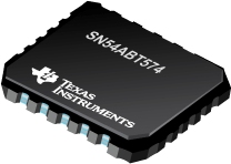
SN54ABT574 - 具有三态输出的八路边沿 D 类触发器
SN54ABT574是TI德州仪器公司的一款D类触发器产品,SN54ABT574是具有三态输出的八路边沿 D 类触发器,本站介绍了SN54ABT574的封装应用图解、特点和优点、功能等,并给出了与SN54ABT574相关的TI元器件型号供参考。
SN54ABT574 - 具有三态输出的八路边沿 D 类触发器 - D类触发器 - 触发器/锁存器/寄存器 - 德州仪器
These 8-bit flip-flops feature 3-state outputs designed specifically for driving highly capacitive or relatively low-impedance loads. They are particularly suitable for implementing buffer registers, I/O ports, bidirectional bus drivers, and working registers.
The eight flip-flops of the SN54ABT574 and SN74ABT574A are edge-triggered D-type flip-flops. On the positive transition of the clock (CLK) input, the Q outputs are set to the logic levels set up at the data (D) inputs.
A buffered output-enable (OE)\ input can be used to place the eight outputs in either a normal logic state (high or low logic levels) or the high-impedance state. In the high-impedance state, the outputs neither load nor drive the bus lines significantly. The high-impedance state and increased drive provide the capability to drive bus lines without need for interface or pullup components.
OE\ does not affect the internal operations of the flip-flops. Old data can be retained or new data can be entered while the outputs are in the high-impedance state.
To ensure the high-impedance state during power up or power down, OE\ should be tied to VCC through a pullup resistor; the minimum value of the resistor is determined by the current-sinking capability of the driver.
This device is fully specified for partial-power-down applications using Ioff. The Ioff circuitry disables the outputs, preventing damaging current backflow through the device when it is powered down.
- Typical VOLP (Output Ground Bounce) <1 V at VCC = 5 V, TA = 25°C
- High-Drive Outputs (–32-mA IOH, 64-mA IOL)
- Ioff Supports Partial-Power-Down Mode Operation
- Latch-Up Performance Exceeds 500 mA Per JEDEC Standard JESD 17
- ESD Protection Exceeds JESD 22
- 2000-V Human-Body Model (A114-A)
- 200-V Machine Model (A115-A)
- TS12A44515 - 低导通电阻四路 SPST CMOS 模拟开关
- LM95214 - 具有 SMBus 接口的 ±2°C 四路远程和本地温度传感器
- SN74AHCT123A - 双路可重触发单稳多频振荡器
- TPS40009 - 低输入 (2.25V-5.5V) 600 kHz 频率同步降压控制器,具有输出驱动/吸入和预偏置操作
- AM4376 - AM437x ARM Cortex-A9 微处理器 (MPU)
- TS3DV416 - 适用于 DVI/HDMI 应用领域的 4 通道差动 8:16 Mux 开关
- TL317 - 3/8 引脚 100mA 可调节正电压稳压器
- SN54HC157-SP - 四路 2 线路至 1 线路数据选择器/多路复用器
- ADC34J22 - 四通道 12 位 50 160 Msps 模数转换器
- TPS826765 - 采用 MicroSiP(tm) 封装的 600mA 完全集成式低噪声降压转换器

