



- BQ20Z80ADBTR-V110 - 集成电路(IC) > 电源管理(PMIC) > 电池管理
- TLC2264AMJB - 集成电路(IC) > 线性 > 放大器 > 仪器,运算放大器,缓冲器
- SN74HCS137PWR - 集成电路(IC) > 逻辑 > 信号开关,多路复用器,解码器
- ADS8556IPMR - 集成电路(IC) > 数据采集 > 模数转换器(ADC)
- DS14C535MSAX - 集成电路(IC) > 接口 > 驱动器,接收器,收发器
- TLC3578EVM - 开发板,套件,编程器 > 评估板 > 模数转换器(ADC)评估板
- ADC10080CIMTX - 集成电路(IC) > 数据采集 > 模数转换器(ADC)
- CC2620F128RGZT - 射频和无线 > 射频收发器 IC
- SN74LVC1G00YEPR - 集成电路(IC) > 逻辑 > 门和反相器
- UCC39002DR - 集成电路(IC) > 电源管理(PMIC) > 电源管理 - 专用
- CD4035BPW - 集成电路(IC) > 逻辑 > 移位寄存器
- TLV0838CDW - 集成电路(IC) > 数据采集 > 模数转换器(ADC)
- LM4912MMBD - 开发板,套件,编程器 > 评估板 > 音频放大器评估板
- SN74LV541ATPWR - 集成电路(IC) > 逻辑 > 缓冲器,驱动器,接收器,收发器
- TLV7111812DSER - 集成电路(IC) > 电源管理(PMIC) > 稳压器 - 线性
- CC1020RSSR - 射频和无线 > 射频收发器 IC
- SN74GTLP817DWRE4 - 逻辑器件 - 转换器,电平移位器
- CDC341DWG4 - 集成电路(IC) > 时钟/定时 > 时钟缓冲器,驱动器
- LM3S9B95-IBZ80-C5 - 集成电路(IC) > 嵌入式 > 微控制器
- ONET1130EPRSMR - 集成电路(IC) > 线性 > 放大器 > 特殊用途放大器



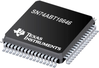
SN74ABT18646 - 具有 18 位总线收发器和寄存器的扫描测试设备
SN74ABT18646是TI德州仪器公司的一款边界扫描(JTAG)逻辑产品,SN74ABT18646是具有 18 位总线收发器和寄存器的扫描测试设备,本站介绍了SN74ABT18646的封装应用图解、特点和优点、功能等,并给出了与SN74ABT18646相关的TI元器件型号供参考。
SN74ABT18646 - 具有 18 位总线收发器和寄存器的扫描测试设备 - 边界扫描(JTAG)逻辑 - 特殊逻辑 - 德州仪器
This scan test device with a 18-bit bus transceiver and register is a member of the Texas Instruments SCOPE™ testability IC family. This device supports IEEE Std 1149.1-1990 boundary scan to facilitate testing of complex circuit board assemblies. Scan access to the test circuitry is accomplished via the four-wire test access port (TAP) interface.
In the normal mode, this device is an 18-bit bus transceiver and register that allows for multiplexed transmission of data directly from the input bus or from the internal registers. It can be used either as two 9-bit transceivers or one 18-bit transceiver. The test circuitry can be activated by the TAP to take snapshot samples of the data appearing at the device pins or to perform a self-test on the boundary test cells. Activating the TAP in the normal mode does not affect the functional operation of the SCOPE bus transceivers and registers.
Transceiver function is controlled by output-enable (OE)\ and direction (DIR) inputs. When (OE)\ is low, the transceiver is active and operates in the A-to-B direction when DIR is high or in the B-to-A direction when DIR is low. When (OE)\ is high, both the A and B outputs are in the high-impedance state, effectively isolating both buses.
Data flow is controlled by clock (CLKAB and CLKBA) and select (SAB and SBA) inputs. Data on the A bus is clocked into the associated registers on the low-to-high transition of CLKAB. When SAB is low, real-time A data is selected for presentation to the B bus (transparent mode). When SAB is high, stored A data is selected for presentation to the B bus (registered mode). The function of the CLKBA and SBA inputs mirrors that of CLKAB and SAB, respectively. Figure 1 illustrates the four fundamental bus-management functions that can be performed with the SN74ABT18646.
In the test mode, the normal operation of the SCOPE bus transceivers and registers is inhibited, and the test circuitry is enabled to observe and control the I/O boundary of the device. When enabled, the test circuitry can perform boundary scan test operations according to the protocol described in IEEE Std 1149.1-1990.
Four dedicated test pins are used to observe and control the operation of the test circuitry: test data input (TDI), test data output (TDO), test mode select (TMS), and test clock (TCK). Additionally, the test circuitry can perform other testing functions, such as parallel signature analysis on data inputs and pseudorandom pattern generation from data outputs. All testing and scan operations are synchronized to the TAP interface.
Additional flexibility is provided in the test mode through the use of two boundary scan cells (BSCs) for each I/O pin. This allows independent test data to be captured and forced at either bus (A or B). A PSA/COUNT instruction is also included to ease the testing of memories and other circuits where a binary count addressing scheme is useful.
- Member of the Texas Instruments Widebus™ Family
- Compatible With IEEE Std 1149.1-1990 (JTAG) Test Access Port and Boundary-Scan Architecture
- Includes D-Type Flip-Flops and Control Circuitry to Provide Multiplexed Transmission of Stored and Real-Time Data
- Two Boundary-Scan Cells Per I/O for Greater Flexibility
- SCOPE™ Instruction Set
- IEEE Std 1149.1-1990 Required Instructions, Optional INTEST, and P1149.1A CLAMP and HIGHZ
- Parallel Signature Analysis at Inputs With Masking Option
- Pseudorandom Pattern Generation From Outputs
- Sample Inputs/Toggle Outputs
- Binary Count From Outputs
- Device Identification
- Even-Parity Opcodes
SCOPE and Widebus are trademarks of Texas Instruments.
- LDC1612 - 具有 I2C 的双通道、28 位电感数字转换器
- UC3851 - 可编程脱机 PWM 控制器
- SN74LVC2G74-Q1 - 汽车类具有清零和预设功能的单路上升沿 D 类触发器
- ISO7842 - 高性能 5.7kVRMS 增强型四通道数字隔离器
- MSP430F5326 - MSP430F532x 混合信号微处理器
- PCM2906C - 具有线性输出和 S/PDIF 的、总线供电的立体声 USB 编解码器
- TMP435 - 具有自动 β、N 因数和串联电阻校正的 ±1°C 远程和本地温度传感器
- SN74LS297 - 数字锁相环滤波器
- TPS2378 - High Efficiency IEEE 802.3at PD Controller with Integrated DC/DC
- LP2985A-30 - 具有关断状态和 1% 容限的 150mA 低噪声低压降稳压器

