


- SN74ACT3G99RKSR - 集成电路(IC) > 逻辑 > 门和反相器 - 多功能,可配置
- LM361MX - 集成电路(IC) > 线性 > 比较器
- LM3S8938-IBZ50-A2T - 嵌入式 - 微控制器
- TPS2220ADBR - 集成电路(IC) > 电源管理(PMIC) > 配电开关,负载驱动器
- SNJ54H11W - 集成电路(IC) > 逻辑 > 门和反相器
- ISOW7842DWE - 隔离器 > 数字隔离器
- SN74AHCT32QDRQ1 - 集成电路(IC) > 逻辑 > 门和反相器
- TPS611781RNWT - 集成电路(IC) > 电源管理(PMIC) > 稳压器 - DC-DC 开关稳压器
- LMH0202MT/NOPB - 集成电路(IC) > 接口 > 专用
- SN75372DR - 集成电路(IC) > 电源管理(PMIC) > 栅极驱动器
- TPSM828223SILR - 板安装电源 > 直流转换器
- CD4031BNSRE4 - 逻辑 - 移位寄存器
- LM5101ASD - 集成电路(IC) > 电源管理(PMIC) > 栅极驱动器
- PCM1702P-KG4 - 集成电路(IC) > 数据采集 > ADC/DAC - 特殊用途
- LM2419T - 集成电路(IC) > 线性 > 放大器 > 视频放大器和模块
- ADS7828EB/250G4 - 集成电路(IC) > 数据采集 > 模数转换器(ADC)
- PTH08T210WAD - 板安装电源 > 直流转换器
- TPS73701DRVR - 集成电路(IC) > 电源管理(PMIC) > 稳压器 - 线性
- OPA317QDBVRQ1 - 集成电路(IC) > 线性 > 放大器 > 仪器,运算放大器,缓冲器
- LMK6DA10000ADLFR - 晶体,振荡器,谐振器 > 振荡器


SN74AVC2T245 - 具有可配置电压转换和三态输出的双位 2-DIR 引脚双电源总线收发器
SN74AVC2T245是TI德州仪器公司的一款无产品,SN74AVC2T245是具有可配置电压转换和三态输出的双位 2-DIR 引脚双电源总线收发器,本站介绍了SN74AVC2T245的封装应用图解、特点和优点、功能等,并给出了与SN74AVC2T245相关的TI元器件型号供参考。
SN74AVC2T245 - 具有可配置电压转换和三态输出的双位 2-DIR 引脚双电源总线收发器 - 无 - 小尺寸逻辑器件 - 德州仪器
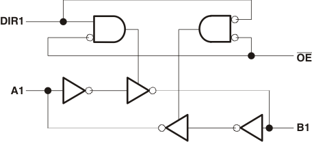
- Each Channel Has Independent Direction Control
- Control Inputs VIH/VIL Levels Are Referenced to VCCA Voltage
- Fully Configurable Dual-Rail Design Allows Each Port to Operate Over the Full 1.2 V to 3.6 V Power-Supply Range
- I/Os Are 4.6 V Tolerant
- Ioff Supports Partial-Power-Down Mode Operation
- VCC Isolation Feature - If Either VCC Input is at GND, Both Ports are in High-Impedance State
- Typical Data Rates
- 500 Mbps (1.8 V to 3.3 V Level-Shifting)
- 320 Mbps (<1.8 V to 3.3 V Level-Shifting)
- 320 Mbps (Translate to 2.5 V or 1.8 V)
- 280 Mbps (Translate to 1.5 V)
- 240 Mbps (Translate to 1.2 V)
- Latch-Up Performance Exceeds 100 mA Per JESD 78, Class II
- ESD Protection Exceeds JESD 22
- 5000 V Human-Body Model (A114-A)
- 200 V Machine Model (A115-A)
- 1500 V Charged-Device Model (C101)
- Personal Electronics
- Industrial
- Enterprise
- Telecom
This dual-bit noninverting bus transceiver uses two separate configurable power-supply rails. The A port is designed to track VCCA. VCCA accepts any supply voltage from 1.2 V to 3.6 V. The B port is designed to track VCCB. VCCB accepts any supply voltage from 1.2 V to 3.6 V. This allows for universal low-voltage bidirectional translation between any of the 1.2 V, 1.5 V, 1.8 V, 2.5 V, and 3.3 V voltage nodes.
The SN74AVC2T245 is designed for asynchronous communication between two data buses. The logic levels of the direction-control (DIR) input and the output-enable (OE) activate either the B-port outputs or the A-port outputs or place both output ports into the high-impedance mode . The device transmits data from the A bus to the B bus when the B-port outputs are activated and from the B bus to the A bus when the A-port outputs are activated. The input circuitry on both A and B ports always is active and must have a logic HIGH or LOW level applied to prevent excess ICC and ICCZ.
The SN74AVC2T245 control pins (DIR1, DIR2, and OE) are supplied by VCCA.
This device is fully specified for partial-power-down applications using Ioff. The Ioff circuitry disables the outputs, preventing damaging current backflow through the device when it is powered down.
The VCC isolation feature ensures that if either VCC input is at GND, both ports are in the high-impedance state.
To ensure the high-impedance state during power up or power down, OE must be connected to VCC through a pull-up resistor; the minimum value of the resistor is determined by the current-sinking capability of the driver.
| PART NUMBER | PACKAGE | BODY SIZE (NOM) |
|---|---|---|
| SN74AVC2T245 | UQFN (10) | 1.80 mm × 1.40 mm |
- SN54ALS373A - 具有三态输出的八路 D 类透明锁存器
- DP83865 - 千兆 PHYTER V 10/100/1000 以太网物理层
- LM237 - 3 引脚 1.5A 可调节负电压稳压器
- LM329 - 精密基准
- LM3549 - High Power Sequential LED Driver
- ADC12DS105 - 具有串行 LVDS 输出的双路 12 位、105 MSPS A/D 转换器
- CD74HCT75 - 高速 CMOS 逻辑双路 2 位双稳态透明锁存器
- DAC5652A - 10 位 275 MSPS 双路数模转换器
- UC1854 - 高功率因子前置稳压器
- CDCV304 - 通用和 PCI-X 1:4 时钟缓冲器

