



- OMAP5910JGDY1R - 集成电路(IC) > 嵌入式 > 微处理器
- OPA2846ID - 集成电路(IC) > 线性 > 放大器 > 仪器,运算放大器,缓冲器
- TLC7524ENG4 - 集成电路(IC) > 数据采集 > 数模转换器(DAC)
- PT6511H - 直流转换器
- OPA4197ID - 集成电路(IC) > 线性 > 放大器 > 仪器,运算放大器,缓冲器
- TPA4860D - 集成电路(IC) > 线性 > 放大器 > 音频放大器
- LP5996SD-1833/NOPB - 集成电路(IC) > 电源管理(PMIC) > 稳压器 - 线性
- TMS320C6455BCTZ8 - 集成电路(IC) > 嵌入式 > DSP(数字信号处理器)
- TPS62040DGQ - 集成电路(IC) > 电源管理(PMIC) > 稳压器 - DC-DC 开关稳压器
- TLC69608RTWR - 集成电路(IC) > 电源管理(PMIC) > LED 驱动器
- SN74LVC74ADRE4 - 集成电路(IC) > 逻辑 > 触发器
- TLV9302IDR - 集成电路(IC) > 线性 > 放大器 > 仪器,运算放大器,缓冲器
- TPS77150DGK - 集成电路(IC) > 电源管理(PMIC) > 稳压器 - 线性
- LMQ66430MA5RXBRQ1 - 集成电路(IC) > 电源管理(PMIC) > 稳压器 - DC-DC 开关稳压器
- TPS23755RJJR - 集成电路(IC) > 电源管理(PMIC) > 以太网供电(PoE)控制器
- TRF0206EVM-CVAL - 开发板,套件,编程器 > 评估板 > 射频评估和开发套件,板
- LM3S6952-IBZ50-A2T - 嵌入式 - 微控制器
- TLC2272CP - 集成电路(IC) > 线性 > 放大器 > 仪器,运算放大器,缓冲器
- PCF8574APWR - 集成电路(IC) > 接口 > I/O 扩展器
- SN74ABT244ADBR - 集成电路(IC) > 逻辑 > 缓冲器,驱动器,接收器,收发器



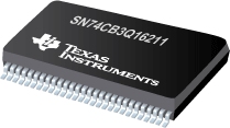
SN74CB3Q16211 - 24 位 FET、2.5V/3.3V、低压高带宽总线开关
SN74CB3Q16211是TI德州仪器公司的一款数字开关产品,SN74CB3Q16211是24 位 FET、2.5V/3.3V、低压高带宽总线开关,本站介绍了SN74CB3Q16211的封装应用图解、特点和优点、功能等,并给出了与SN74CB3Q16211相关的TI元器件型号供参考。
SN74CB3Q16211 - 24 位 FET、2.5V/3.3V、低压高带宽总线开关 - 数字开关 - 信号开关 - 德州仪器
The SN74CB3Q16211 is a high-bandwidth FET bus switch utilizing a charge pump to elevate the gate voltage of the pass transistor, providing a low and flat ON-state resistance (ron). The low and flat ON-state resistance allows for minimal propagation delay and supports rail-to-rail switching on the data input/output (I/O) ports. The device also features low data I/O capacitance to minimize capacitive loading and signal distortion on the data bus. Specifically designed to support high-bandwidth applications, the SN74CB3Q16211 provides an optimized interface solution ideally suited for broadband communications, networking, and data-intensive computing systems.
The SN74CB3Q16211 is organized as two 12-bit bus switches with separate output-enable (1OE\, 2OE\) inputs. It can be used as two 12-bit bus switches or as one 24-bit bus switch. When OE\ is low, the associated 12-bit bus switch is ON and the A port is connected to the B port, allowing bidirectional data flow between ports. When OE\ is high, the associated 12-bit bus switch is OFF, and a high-impedance state exists between the A and B ports.
This device is fully specified for partial-power-down applications using Ioff. The Ioff circuitry prevents damaging current backflow through the device when it is powered down.
To ensure the high-impedance state during power up or power down, OE\ should be tied to VCC through a pullup resistor; the minimum value of the resistor is determined by the current-sinking capability of the driver.
- Member of the Texas Instruments Widebus™ Family
- High-Bandwidth Data Path (Up To 500 MHz)
- 5-V Tolerant I/Os with Device Powered Up or Powered Down
- Low and Flat ON-State Resistance (ron) Characteristics Over Operating Range (ron = 5 Typical)
- Rail-to-Rail Switching on Data I/O Ports
- 0-V to 5-V Switching With 3.3-V VCC
- 0-V to 3.3-V Switching With 2.5-V VCC
- Bidirectional Data Flow, With Near-Zero Propagation Delay
- Low Input/Output Capacitance Minimizes Loading and Signal Distortion (Cio(OFF) = 4 pF Typical)
- Fast Switching Frequency (fOE\ = 20 MHz Max)
- Data and Control Inputs Provide Undershoot Clamp Diodes
- Low Power Consumption (ICC = 1 mA Typical)
- VCC Operating Range From 2.3 V to 3.6 V
- Data I/Os Support 0-V to 5-V Signaling Levels (0.8 V, 1.2 V, 1.5 V, 1.8 V, 2.5 V, 3.3 V, 5 V)
- Control Inputs Can be Driven by TTL or 5-V/3.3-V CMOS Outputs
- Ioff Supports Partial-Power-Down Mode Operation
- Latch-Up Performance Exceeds 100 mA Per JESD 78, Class II
- ESD Performance Tested Per JESD 22
- 2000-V Human-Body Model (A114-B, Class II)
- 1000-V Charged-Device Model (C101)
- Supports Both Digital and Analog Applications: PCI Interface, Differential Signal Interface, Memory Interleaving, Bus Isolation, Low-Distortion Signal Gating
For additional information regarding the performance characteristics of the CB3Q family, refer to the TI application report, CBT-C, CB3T, and CB3Q Signal-Switch Families, literature number SCDA008. Widebus is a trademark of Texas Instruments.
- MAX3232E-Q1 - 具有 +/-15kV ESD 保护的 3V 至 5.5V 多通道 RS-232 线路驱动器/接收器
- DAC8552 - DAC8552:16 位双路电压输出数模转换器
- TPS65800 - 集成单节锂离子电池和电源管理 IC (PMIC)
- CD4053B-MIL - 具有逻辑电平转换功能的 CMOS 三路 2 通道模拟多路复用器/多路解复用器
- ADS7946 - 14 位、2MSPS、双通道、单极、伪差动、u-Power SAR ADC
- SN54LS377 - 具有使能端的八路 D 类触发器
- SN54HC08-SP - 四路 2 输入正与门
- CDC516 - 具有三态输出的 3.3V 锁相环时钟驱动器
- ADS1254-EP - 增强型产品 24 位 20kHz 低功耗模数转换器
- ADS7812 - 低功耗串行 12 位采样模数转换器

