



- AMC1411DWLR - 集成电路(IC) > 线性 > 放大器 > 特殊用途放大器
- TIBPAL16R6-5CN - 嵌入式 - PLD(可编程逻辑器件)
- BQ24715RGRR - 集成电路(IC) > 电源管理(PMIC) > 电池充电器
- SN74LVC125APWRE4 - 集成电路(IC) > 逻辑 > 缓冲器,驱动器,接收器,收发器
- 74CBTH16211DGVRG4 - 逻辑 - 信号开关,多路复用器,解码器
- CD74HC00EE4 - 集成电路(IC) > 逻辑 > 门和反相器
- SN74ALS175DR - 集成电路(IC) > 逻辑 > 触发器
- TMDX570LS30376USCB - 开发板,套件,编程器 > 评估板 > 嵌入式 MCU、DSP 评估板
- TPS2090DG4 - 集成电路(IC) > 电源管理(PMIC) > 配电开关,负载驱动器
- TLV75512PDQNR - 集成电路(IC) > 电源管理(PMIC) > 稳压器 - 线性
- LM3S1162-IQC50-A2 - 集成电路(IC) > 嵌入式 > 微控制器
- UC2876N - 集成电路(IC) > 电源管理(PMIC) > AC DC 转换器,离线开关
- BQ2060SS-E411TRG4 - 集成电路(IC) > 电源管理(PMIC) > 电池管理
- RR-IDISC-PR-USB - RFID 读取器模块
- TPS43335EVM - 开发板,套件,编程器 > 评估板 > DC/DC 和 AC/DC(离线)SMPS 评估板
- SN74HC253NSR - 集成电路(IC) > 逻辑 > 信号开关,多路复用器,解码器
- LP38690SDX-5.0/NOPB - 集成电路(IC) > 电源管理(PMIC) > 稳压器 - 线性
- TPA741DGN - 集成电路(IC) > 线性 > 放大器 > 音频放大器
- MAX3232IDR - 集成电路(IC) > 接口 > 驱动器,接收器,收发器
- TPS54291EVM-431 - 开发板,套件,编程器 > 评估板 > DC/DC 和 AC/DC(离线)SMPS 评估板



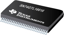
SN74GTL16616 - 具有缓冲时钟输出的 17 位 LVTTL 到 GTL/GTL+ 通用总线收发器
SN74GTL16616是TI德州仪器公司的一款无产品,SN74GTL16616是具有缓冲时钟输出的 17 位 LVTTL 到 GTL/GTL+ 通用总线收发器,本站介绍了SN74GTL16616的封装应用图解、特点和优点、功能等,并给出了与SN74GTL16616相关的TI元器件型号供参考。
SN74GTL16616 - 具有缓冲时钟输出的 17 位 LVTTL 到 GTL/GTL+ 通用总线收发器 - 无 - 背板逻辑器件(GTL/TTL/BTL/ECL收发器/转换器) - 德州仪器
The SN74GTL16616 is a 17-bit UBT™ transceiver that provides LVTTL-to-GTL/GTL+ and GTL/GTL+-to-LVTTL signal-level translation. Combined D-type flip-flops and D-type latches allow for transparent, latched, clocked, and clocked-enabled modes of data transfer identical to the '16601 function. Additionally, this device provides for a copy of CLKAB at GTL/GTL+ signal levels (CLKOUT) and conversion of a GTL/GTL+ clock to LVTTL logic levels (CLKIN). This device provides an interface between cards operating at LVTTL logic levels and a backplane operating at GTL/GTL+ signal levels. Higher-speed operation is a direct result of the reduced output swing (<1 V), reduced input threshold levels, and OEC™ circuitry.
The user has the flexibility of using this device at either GTL (VTT = 1.2 V and VREF = 0.8 V) or the preferred higher noise margin GTL+ (VTT = 1.5 V and VREF = 1 V) signal levels. GTL+ is the Texas Instruments derivative of the Gunning Transceiver Logic (GTL) JEDEC standard JESD 8-3. The B port normally operates at GTL or GTL+ signal levels, while the A-port and control inputs are compatible with LVTTL logic levels and are 5-V tolerant. V REF is the reference input voltage for the B port. VCC (5 V) supplies the internal and GTL circuitry while VCC (3.3 V) supplies the LVTTL output buffers.
Data flow in each direction is controlled by output-enable (OEAB\ and OEBA\), latch-enable (LEAB and LEBA), and clock (CLKAB and CLKBA) inputs. The clock can be controlled by the clock-enable (CEAB\ and CEBA\) inputs. For A-to-B data flow, the device operates in the transparent mode when LEAB is high. When LEAB is low, the A data is latched if CEAB\ is low and CLKAB is held at a high or low logic level. If LEAB is low, the A-bus data is stored in the latch/flip-flop on the low-to-high transition of CLKAB if CEAB\ also is low. When OEAB\ is low, the outputs are active. When OEAB\ is high, the outputs are in the high-impedance state. Data flow for B to A is similar to that of A to B, but uses OEBA\, LEBA, CLKBA, and CEBA\.
This device is fully specified for partial-power-down applications using Ioff. The Ioff circuitry disables the outputs, preventing damaging current backflow through the device when it is powered down.
Active bus-hold circuitry holds unused or undriven LVTTL inputs at a valid logic state. Use of pullup or pulldown resistors with the bus-hold circuitry is not recommended.
To ensure the high-impedance state during power up or power down, OE\ should be tied to VCC through a pullup resistor; the minimum value of the resistor is determined by the current-sinking capability of the driver.
- Member of Texas Instruments' Widebus™ Family
- UBT™ Transceiver Combines D-Type Latches and D-Type Flip-Flops for Operation in Transparent, Latched, Clocked, or Clock-Enabled Modes
- OEC™ Circuitry Improves Signal Integrity and Reduces Electromagnetic Interference
- GTL Buffered CLKAB Signal (CLKOUT)
- Translates Between GTL/GTL+ Signal Levels and LVTTL Logic Levels
- Supports Mixed-Mode (3.3 V and 5 V) Signal Operation on A-Port and Control Inputs
- Equivalent to \x9216601 Function
- Ioff Supports Partial-Power-Down Mode Operation
- Bus Hold on Data Inputs Eliminates the Need for External Pullup/Pulldown Resistors on A Port
- Distributed VCC and GND Pins Minimize High-Speed Switching Noise
- Latch-Up Performance Exceeds 100 mA Per JESD 78, Class II
- ESD Protection Exceeds JESD 22
- 2000-V Human-Body Model (A114-A)
OEC, UBT, and Widebus are trademarks of Texas Instruments.
- SM72485 - SolarMagic 100V, 150 mA Constant On-Time Buck Switching Regulator
- DS1487 - 低功耗 RS-485/1/4 单元负载多点收发器
- TPS62746 - 采用 WCSP 封装且具有负载开关的超低功耗直流-直流转换器
- SN54AS573A - 具有三态输出的八路 D 类透明锁存器
- LM25576 - SIMPLE SWITCHER? 42V,3A 降压开关稳压器
- TAS5613A - 15W 立体声/300W 单声道 PurePath HD 模拟输入功率级
- BQ24745 - 具有输入电流检测比较器的 SMBus 控制的 2 级多化合物电池充电器
- SN54157 - 四路 2 线路至 1 线路数据选择器/多路复用器
- OMAP4430 - OMAP? 4 移动应用平台
- UCC29900 - 完整周期控制器

