


- CD74HCT02E - 集成电路(IC) > 逻辑 > 门和反相器
- REF5025AIDR - 集成电路(IC) > 电源管理(PMIC) > 电压基准
- LM2781TPX/NOPB - 集成电路(IC) > 电源管理(PMIC) > 稳压器 - DC-DC 开关稳压器
- TPS22941DCKR - 集成电路(IC) > 电源管理(PMIC) > 配电开关,负载驱动器
- THVD2412VDR - 集成电路(IC) > 接口 > 驱动器,接收器,收发器
- ADS1672IPAGRG4 - 集成电路(IC) > 数据采集 > 模数转换器(ADC)
- F28P559SJ2PMRQ1 - 集成电路(IC) > 嵌入式 > 微控制器
- COP8CBR9IMT8/NOPB - 集成电路(IC) > 嵌入式 > 微控制器
- SN74AHCT164PWR - 集成电路(IC) > 逻辑 > 移位寄存器
- TRS3232CPWRG4 - 集成电路(IC) > 接口 > 驱动器,接收器,收发器
- TPS2420EVM-01 - 开发板,套件,编程器 > 评估板 > 评估和演示板及套件
- TPS563210ADDFT - 集成电路(IC) > 电源管理(PMIC) > 稳压器 - DC-DC 开关稳压器
- OPA2743EA/2K5 - 集成电路(IC) > 线性 > 放大器 > 仪器,运算放大器,缓冲器
- PTMA402050N2AST - 板安装电源 > 直流转换器
- VSP1021PFB - 集成电路(IC) > 数据采集 > 模拟前端(AFE)
- TM4C1292NCPDTI3R - 集成电路(IC) > 嵌入式 > 微控制器
- ADC08038CIWMX - 集成电路(IC) > 数据采集 > 模数转换器(ADC)
- LM43601QPWPTQ1 - 集成电路(IC) > 电源管理(PMIC) > 稳压器 - DC-DC 开关稳压器
- TPS3808G15DRVR - 集成电路(IC) > 电源管理(PMIC) > 监控器
- LM3S2B93-IBZ80-C3 - 嵌入式 - 微控制器


SN74LVC2G125 - 具有三态输出的双总线缓冲器闸
SN74LVC2G125是TI德州仪器公司的一款TI芯片产品,SN74LVC2G125是具有三态输出的双总线缓冲器闸,本站介绍了SN74LVC2G125的封装应用图解、特点和优点、功能等,并给出了与SN74LVC2G125相关的TI元器件型号供参考。
SN74LVC2G125 - 具有三态输出的双总线缓冲器闸 - TI芯片 - 小尺寸逻辑器件 - 德州仪器
- Available in the Texas Instruments NanoFree™ Package
- Supports 5-V VCC Operation
- Inputs Accept Voltages to 5.5 V
- Max tpd of 4.3 ns at 3.3 V
- Low Power Consumption, 10-µA Max ICC
- ±24-mA Output Drive at 3.3 V
- Typical VOLP (Output Ground Bounce) < 0.8 V at VCC = 3.3 V, TA = 25°C
- Typical VOHV (Output VOH Undershoot) > 2 V at VCC = 3.3 V, TA = 25°C
- Ioff Supports Live Insertion, Partial-Power-Down Mode, and Back-Drive Protection
- Can Be Used as a Down Translator to Translate Inputs From a Max of 5.5 V Down to the VCC Level
- Latch-Up Performance Exceeds 100 mA Per JESD 78, Class II
- ESD Protection Exceeds JESD 22
- 2000-V Human-Body Model
- 200-V Machine Model
- 1000-V Charged-Device Model
- Cable Modem Termination Systems
- High-Speed Data Acquisition and Generation
- Military: Radars and Sonars
- Motor Controls: High-Voltage
- Power Line Communication Modems
- SSDs: Internal or External
- Video Broadcasting and Infrastructure: Scalable Platforms
- Video Broadcasting: IP-Based Multi-Format Transcoders
- Video Communications Systems
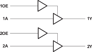
The SN74LVC2G125 device is a dual bus buffer gate, designed for 1.65-V to 5.5-V VCC operation. This device features dual line drivers with 3-state outputs. The outputs are disabled when the associated output-enable (OE) input is high.
NanoFree™ package technology is a major breakthrough in IC packaging concepts, using the die as the package.
To ensure the high-impedance state during power up or power down, OE should be tied to VCC through a pullup resistor; the minimum value of the resistor is determined by the current-sinking capability of the driver.
This device is fully specified for partial-power-down applications using Ioff. The Ioff circuitry disables the outputs, preventing damaging current backflow through the device when it is powered down.
| PART NUMBER | PACKAGE | BODY SIZE |
|---|---|---|
| SN74LVC2G125 | SM8 (8) | 2.95 mm × 2.80 mm |
| US8 (8) | 2.30 mm × 2.00 mm | |
| DSBGA (8) | 1.91 mm × 0.91 mm |
- TS5L100 - 具有低导通电阻的四路 SPDT 宽带网络开关
- ADS6129 - 低功耗 12 位 250MSPS ADC
- CD74HCT154 - 高速 CMOS 逻辑 4 至 16 线路解码器/多路解复用器
- SN74AUP3G14 - 低功耗三路施密特触发反向器
- SN74ALVCH16821 - 具有三态输出的 3.3V 20 位总线接口触发器
- LM2682 - 开关电容器倍压逆变器
- MSP430FR69721 - MSP430FR697x(1)、MSP430FR6 87x(1)、MSP430FR692x(1)、MSP430FR682x(1) MCU
- BQ2947 - 可提供精确逐电池电压监视的锂离子保护 IC 系列
- SN74LVC02A-EP - 增强型产品四路 2 输入正或非门
- MSP430F5333 - MSP430F533x 混合信号微处理器

