



- DM54LS125AJ/883 - 集成电路(IC) > 逻辑 > 缓冲器,驱动器,接收器,收发器
- ESD2CAN24DCKRQ1 - 电路保护 > 瞬态电压抑制器(TVS) > TVS 二极管
- LMH1297EVM - 开发板,套件,编程器 > 评估板 > 评估和演示板及套件
- TPS23751EVM-104 - 开发板,套件,编程器 > 评估板 > DC/DC 和 AC/DC(离线)SMPS 评估板
- OMAPL137BZKBD4 - 集成电路(IC) > 嵌入式 > 微处理器
- DS90UB947NTRGCTQ1 - 接口 - 串行器,解串器
- AM1707CZKBD4 - 集成电路(IC) > 嵌入式 > 微处理器
- TPS61282YFFR - 集成电路(IC) > 电源管理(PMIC) > 稳压器 - DC-DC 开关稳压器
- DRV8410EVM - 开发板,套件,编程器 > 评估板 > 评估和演示板及套件
- LP2967IMM-2828/NOPB - 电源管理IC - 稳压器 - 线性
- CD74HC241M - 集成电路(IC) > 逻辑 > 缓冲器,驱动器,接收器,收发器
- TMS5701225BPGEQQ1 - 集成电路(IC) > 嵌入式 > 微控制器
- SN75114DRG4 - 接口 - 驱动器,接收器,收发器
- TLC25L2CPSRG4 - 集成电路(IC) > 线性 > 放大器 > 仪器,运算放大器,缓冲器
- SN74HCT02NG4 - 集成电路(IC) > 逻辑 > 门和反相器
- OPA227PA - 集成电路(IC) > 线性 > 放大器 > 仪器,运算放大器,缓冲器
- TLE2425IDR - 集成电路(IC) > 电源管理(PMIC) > 电压基准
- UCC3808AD-1 - 集成电路(IC) > 电源管理(PMIC) > DC-DC 开关控制器
- SN75LBC176P - 集成电路(IC) > 接口 > 驱动器,接收器,收发器
- TPS72012YZUR - 集成电路(IC) > 电源管理(PMIC) > 稳压器 - 线性



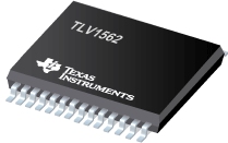
TLV1562 - 10 位四通道(可配置)2MSPS ADC,具有多路可编程分辨率与速度/转换模式,自动工作
TLV1562是TI德州仪器公司的一款精密ADC(<=10MSPS)产品,TLV1562是10 位四通道(可配置)2MSPS ADC,具有多路可编程分辨率与速度/转换模式,自动工作,本站介绍了TLV1562的封装应用图解、特点和优点、功能等,并给出了与TLV1562相关的TI元器件型号供参考。
TLV1562 - 10 位四通道(可配置)2MSPS ADC,具有多路可编程分辨率与速度/转换模式,自动工作 - 精密ADC(<=10MSPS) - 模数转换器 - 德州仪器
The TLV1562 is a 10-bit CMOS low-power, high-speed programmable resolution analog-to-digital converter based on a low-power recyclic architecture. The unique architecture delivers a throughput up to 2 MSPS (million samples per second) at 10-bit resolution. The programmable resolution allows a higher conversion throughput as a tradeoff of lower resolution. A high speed 3-state parallel port directly interfaces to a digital signal processor (DSP) or microprocessor (uP) system data bus. D0 through D9 are the digital output terminals with D0 being the least significant bit (LSB). The TLV1562 is designed to operate for a wide range of supply voltages (2.7 V to 5.5 V) with very low power consumption (11 mA maximum at 5.5 V, 10 MHz CLKIN). The power saving feature is further enhanced with a software power-down feature (1 uA maximum) and auto power-down (1 uA maximum) feature.
Many programmable features make this device a flexible general-purpose data converter. The device can be configured as either four single-ended inputs to maximize the capacity or two differential inputs to improve noise immunity. The internal system clock (SYSCLK) may come from either an internally generated OSC or an external clock source (CLKIN). Four different modes of conversion are available for different applications. The interrupt driven modes are mostly suitable for asynchronous applications, while the continuous modes take advantage of the high speed nature of a pipelined architecture. A pair of built-in sample-and-hold amplifiers allow simultaneous sampling of two input channels. This makes the TLV1562 perfect for communication applications. Conversion is started by the RD\ signal, which can also be used for reading data, to maximize the throughput. Conversion can be started either by the RD\ or CSTART\ signal when the device is operating in the interrupt-driven modes. The dedicated conversion start pin, CSTART\, provides a mechanism to simultaneously sample and convert multiple channels when multiple converters are used in an application.
The converter incorporates a pair of differential high-impedance reference inputs that facilitate ratiometric conversion, scaling, and isolation of analog circuitry from logic and supply noise. Other features such as low input capacitance (10 pF) and very wide input bandwidth (75 MHz) make this device a perfect digital signal processing (DSP) companion for mobile communication applications. A switched-capacitor design allows low-error conversion over the full operating free-air temperature range.
The features that make this device truly a DSP friendly converter include: 1) programmable continuous conversion modes, 2) programmable 2s complement output code format, and 3) programmable resolution. The TLV1562 is offered in both 28-pin TSSOP and SOIC packages. The TLV1562C is characterized for operation from 0°C to 70°C. The TLV1562I is characterized for operation over the full industrial temperature range of -40°C to 85°C.
- 2 MSPS Max Throughput at 10 Bit (Single Channel), ±1 LSB DNL, ±1 LSB INL MAX
- 3 MSPS Max Throughput at 8 Bit (Single Channel), ±1 LSB DNL, ±1 LSB INL MAX
- 7 MSPS Max Throughput at 4 Bit (Single Channel), ±0.4 LSB DNL, ±0.4 LSB INL MAX
- No Missing Code for External Clock Up to 15 MHz at 5.5 V, 12 MHz at 2.7 V
- ENOB 9.4 Bit, SINAD 57.8 dB, SFDR -70.8 dB, THD -68.8 dB, at fi = 800 kHz, 10 Bit
- Wide Input Bandwidth for Undersampling (75 MHz at 1 dB, >120 MHz at -3 dB) at Rs = 1 k
- Software Programmable Power Down, (1 uA), Auto Powerdown (120 uA)
- Single Wide Range Supply 2.7 VDC to 5.5 VDC
- Low Supply Current 11 mA at 5.5 V, 10 MHz; 7 mA at 2.7 V, 8 MHz Operating
- Simultaneous Sample and Hold:
- Dual Sample and Hold Matched Channels
- Multi Chip Simultaneous Sample and Hold Capable
- Programmable Conversion Modes: Interrupt-Driven for Shorter Latency Continuous Modes Optimized for MIPS Sensitive DSP Solutions
- Built-In Internal/System Mid-Scale Error Calibration
- Built-In Mux With 2 Differential or 4 Single-Ended Input Channels
- Low Input Capacitance (10 pF Max Fixed, 1 pF Max Switching)
- DSP/u P-Compatible Parallel Interface
- TIBPAL20R4-20M - 高性能 Impact PAL 电路
- ADS7954 - 10 位、1MSPS、4 通道、单端、微功耗、串行接口、SAR ADC
- SN65LBC171 - 三路差动收发器
- UCD7100 - 具有电流感应的数字控制兼容单输出低侧 +/- 4A MOSFET 驱动器
- PCM2906C - 具有线性输出和 S/PDIF 的、总线供电的立体声 USB 编解码器
- CDC204 - 5V 6 位反向器/时钟驱动器
- UC2856Q - 改进的电流模式 PWM 控制器
- TLK2218 - TLK2218:8 端口千兆以太网收发器
- CD54HCT75 - 高速 CMOS 逻辑双路 2 位双稳态透明锁存器
- TPS65132 - 用于显示的双极电源

