


- OPA187IDGKR - 集成电路(IC) > 线性 > 放大器 > 仪器,运算放大器,缓冲器
- LP5900TL-2.2/NOPB - 集成电路(IC) > 电源管理(PMIC) > 稳压器 - 线性
- TLV2252IP - 集成电路(IC) > 线性 > 放大器 > 仪器,运算放大器,缓冲器
- TPS65141RGER - 集成电路(IC) > 电源管理(PMIC) > 电源管理 - 专用
- TPS62177DQCT - 集成电路(IC) > 电源管理(PMIC) > 稳压器 - DC-DC 开关稳压器
- SN74ACT573DBR - 集成电路(IC) > 逻辑 > 锁存器
- TLV5638IDRG4 - 集成电路(IC) > 数据采集 > 数模转换器(DAC)
- LM4050BEM3-5.0 - 集成电路(IC) > 电源管理(PMIC) > 电压基准
- LMV341MGX - 集成电路(IC) > 线性 > 放大器 > 仪器,运算放大器,缓冲器
- LF198AH/NOPB - 集成电路(IC) > 线性 > 放大器 > 仪器,运算放大器,缓冲器
- TPS78925DBVTG4 - 集成电路(IC) > 电源管理(PMIC) > 稳压器 - 线性
- TPS65273VTEVM - 开发板,套件,编程器 > 评估板 > DC/DC 和 AC/DC(离线)SMPS 评估板
- TPS62007DGSR - 集成电路(IC) > 电源管理(PMIC) > 稳压器 - DC-DC 开关稳压器
- REF3112AIDBZR - 集成电路(IC) > 电源管理(PMIC) > 电压基准
- INA205AID - 集成电路(IC) > 电源管理(PMIC) > 电流调节/管理
- TPS65090ARVNT - 集成电路(IC) > 电源管理(PMIC) > 电池充电器
- TB3R2DG4 - 接口 - 驱动器,接收器,收发器
- SM72480SD-120/NOPB - 传感器,变送器 > 温度传感器 > 温控器 - 固态
- THS7316D - 集成电路(IC) > 线性 > 放大器 > 视频放大器和模块
- M0G3507QRHBRQ1 - 集成电路(IC) > 嵌入式 > 微控制器


TPS650842 - 用于 Braswell 处理器的可编程宽输入电压范围电源管理 IC (PMIC)
TPS650842是TI德州仪器公司的一款TI芯片产品,TPS650842是用于 Braswell 处理器的可编程宽输入电压范围电源管理 IC (PMIC),本站介绍了TPS650842的封装应用图解、特点和优点、功能等,并给出了与TPS650842相关的TI元器件型号供参考。
TPS650842 - 用于 Braswell 处理器的可编程宽输入电压范围电源管理 IC (PMIC) - TI芯片 - 电源管理多通道IC(PMIC)解决方案 - 德州仪器
- Three Variable-Output Voltage Step-Down Controllers
- Wide VIN Range From 5.4 V to 21 V
- Up to 7-A Output Current for BUCK1 (VCC) and BUCK6 (VDDQ), and 11-A for BUCK2 (VGG) Using External FETs
- I2C DVS Control (0.5 V to 1.45 V in 10-mV Steps) for BUCK1 and BUCK2
- Pin-Selectable Dual Output Voltages (1.2 V or 1.35 V) for BUCK6 (VDDQ)
- Three Variable-Output Voltage Synchronous Step-Down Converters
- VIN Range From 4.5 V to 5.5 V
- Up to 3.5 A of Output Current for BUCK3 (VNN) With I2C DVS Control (0.65 V to 1.45 V in 25-mV Steps)
- Up to 3 A of Output Current for BUCK4 (V1P05A) and up to 1.5 A of Output Current for BUCK5 (V1P8A)
- Three LDO Regulators With Adjustable Output Voltage
- LDOA1: I2C-Selectable Output Voltage From 1.35 V to 3.3 V for up to 200 mA of Output Current
- LDOA2: I2C-Selectable Output Voltage From 1.05 V, 1.1 V, 1.15 V, and 1.2 V
- LDOA3: I2C-Selectable Output Voltage From 1.1 V, 1.15 V, 1.2 V, and 1.24 V
- VTT LDO for DDR3 and DDR4 Memory Termination
- Three Load Switches With Slew Rate Control
- Up to 300 mA of Output Current With Voltage Drop Less Than 1.5% of Nominal Input Voltage
- RDSON < 96 mΩ at Input Voltage of 1.8 V
- I2C Interface (Device Address 0x5E) Supports Standard Mode (100 kHz), Fast Mode (400 kHz), and Fast Mode Plus (1 MHz)
- 64-Pin, Single-Row, 0.4-mm Pitch QFN Package
- 2-, 3-, or 4-Series Cell Li-Ion Battery Powered Products (NVDC or Non-NVDC)
- Tablet, Ultrabook, and Notebook Computers
- Mobile PCs and Mobile Internet Devices
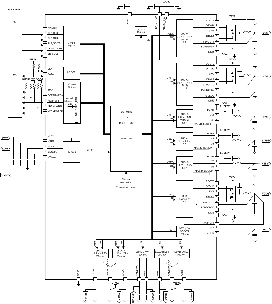
The TPS650842 device is a single-chip solution, power-management IC designed specifically for the latest Intel™ processors targeted for tablets, ultrabooks, and notebooks with NVDC or non-NVDC power architectures, using 2S, 3S, or 4S Li-Ion battery packs. The TPS650842 device is used for essential systems with low-voltage rails merged for the smallest footprint and lowest-cost system-power solution. The TPS650842 device provides the complete power solution based on the Intel Reference Designs. Six highly efficient step-down voltage regulators (VRs), a sink or source LDO (VTT), two LDOs, and three load switches are controlled by power-up sequence logic to provide the proper power rails, sequencing, and protection—including DDR3 and DDR4 memory power. The three regulators (BUCK1–BUCK3) support dynamic voltage scaling (DVS) for maximum efficiency—including support for Connected Standby. The high-frequency VRs use small inductors and capacitors to achieve a small solution size. An I2C interface allows simple control by an embedded controller (EC) or by a system on chip (SoC). The PMIC comes in an 8-mm × 8-mm single-row QFN package with a thermal pad for good thermal dissipation and ease of board routing.
Use the following email address to request the full version of this data sheet: ipgmkt@list.ti.com.
| PART NUMBER | PACKAGE | BODY SIZE (NOM) |
|---|---|---|
| TPS650842 | RSK (64) | 8.00 mm × 8.00 mm |
- UC2714 - 辅助开关 FET 驱动器
- CD4027B - CMOS 双路 J-K 主/从触发器
- TPS76833-EP - 增强型产品快速瞬态响应 1A 低压降稳压器
- TPS60401 - 具有固定 20kHz 操作的 60mA 充电泵电压反向器
- LM5008A - 100V、350mA 宽输入电压恒定导通时间降压开关稳压器
- BQ771604 - 用于 2 至 4 节锂离子电池(具有外部延迟电容器)的过压保护
- SN74ALS257A - 具有三态输出的四路 2 线路至 1 线路数据选择器/多路复用器
- CC8531 - 用于无线数字音频流的 PurePath? 无线 2.4GHz 射频 SoC
- UC2856-Q1 - 汽车类改进的电流模式 PWM 控制器
- SN55976A - 9 通道差动收发器

