



- SN75110AN - 集成电路(IC) > 接口 > 驱动器,接收器,收发器
- F280023PTQR - 集成电路(IC) > 嵌入式 > 微控制器
- DEM-FDA-RUN-EVM - 开发板,套件,编程器 > 评估板 > 运算放大器评估板
- RES60EVM - 开发板,套件,编程器 > 评估板 > 评估和演示板及套件
- ADC08351CIMTCX - 集成电路(IC) > 数据采集 > 模数转换器(ADC)
- TPS92314DR/NOPB - 集成电路(IC) > 电源管理(PMIC) > LED 驱动器
- OPA2134UAG4 - 集成电路(IC) > 线性 > 放大器 > 仪器,运算放大器,缓冲器
- CSD19532KTT - 分立半导体产品 > 晶体管 > FET,MOSFET > 单 FET,MOSFET
- LM4838LQX/NOPB - 集成电路(IC) > 线性 > 放大器 > 音频放大器
- LM4050BIM3X-4.1/NOPB - 集成电路(IC) > 电源管理(PMIC) > 电压基准
- TMS320VC5470GHK - 集成电路(IC) > 嵌入式 > DSP(数字信号处理器)
- LP38692MP-1.8 - 集成电路(IC) > 电源管理(PMIC) > 稳压器 - 线性
- LM8365BALMFX45/NOPB - 集成电路(IC) > 电源管理(PMIC) > 监控器
- LM2698MM-ADJ/NOPB - 集成电路(IC) > 电源管理(PMIC) > 稳压器 - DC-DC 开关稳压器
- SN74S174N - 集成电路(IC) > 逻辑 > 触发器
- AM3354BZCEA30 - 嵌入式 - 微处理器
- BQ2084DBT - 集成电路(IC) > 电源管理(PMIC) > 电池管理
- TPA701DGNR - 集成电路(IC) > 线性 > 放大器 > 音频放大器
- TPS53119EVM-690 - 开发板,套件,编程器 > 评估板 > DC/DC 和 AC/DC(离线)SMPS 评估板
- TMP302DQDRLRQ1 - 传感器,变送器 > 温度传感器 > 温控器 - 固态



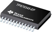
TPS70345-EP - 具有加电定序的增强型产品双路输出低压降稳压器
TPS70345-EP是TI德州仪器公司的一款多通道LDO产品,TPS70345-EP是具有加电定序的增强型产品双路输出低压降稳压器,本站介绍了TPS70345-EP的封装应用图解、特点和优点、功能等,并给出了与TPS70345-EP相关的TI元器件型号供参考。
TPS70345-EP - 具有加电定序的增强型产品双路输出低压降稳压器 - 多通道LDO - 线性稳压器(LDO) - 德州仪器
The TPS70345 is designed to provide a complete power management solution for Texas Instruments DSP, processor power, ASIC, FPGA, and digital applications where dual output voltage regulators are required. Easy programmability of the sequencing function makes this family ideal for any Texas Instruments DSP applications with power sequencing requirement. Differentiated features, such as accuracy, fast transient response, SVS supervisory circuit (power on reset), manual reset inputs, and enable function, provide a complete system solution.
The TPS70345 voltage regulator offers low dropout voltage and dual outputs with power up sequence control, which is designed primarily for DSP applications. This device has a low noise output performance without using any added filter bypass capacitors and are designed to have a fast transient response and be stable with 47 µF low ESR capacitors.
This device has a fixed output voltage 3.3 V/1.2 V. Regulator 1 can support up to 1 A, and regulator 2 can support up to 2 A. Separate voltage inputs allow the designer to configure the source power.
Because the PMOS pass element behaves as a low-value resistor, the dropout voltage is very low (typically 160 mV on regulator 1) and is directly proportional to the output current. Additionally, since the PMOS pass element is a voltage-driven device, the quiescent current is low and independent of output loading (maximum of 250 µA over the full range of output current). This LDO family also features a sleep mode; applying a high signal to EN\ (enable) shuts down both regulators, reducing the input current to 1 µA at TJ = 25°C.
The device is enabled when the EN\ pin is connected to a low-level input voltage. The output voltages of the two regulators are sensed at the VSENSE1 and VSENSE2 pins respectively.
The input signal at the SEQ pin controls the power-up sequence of the two regulators. When the device is enabled and the SEQ terminal is pulled high or left open, VOUT2 turns on first and VOUT1 remains off until VOUT2 reaches approximately 83% of its regulated output voltage. At that time VOUT1 is turned on. If VOUT2 is pulled below 83% (i.e. overload condition) of its regulated voltage, VOUT1 will be turned off. Pulling the SEQ terminal low reverses the power-up order and VOUT1 is turned on first. The SEQ pin is connected to an internal pullup current source.
For each regulator, there is an internal discharge transistor to discharge the output capacitor when the regulator is turned off (disabled).
The PG1 pin reports the voltage conditions at VOUT1. The PG1 pin can be used to implement a SVS (power on reset) for the circuitry supplied by regulator 1.
The TPS70345 features a RESET (SVS, POR, or power on reset). RESET\ is an active low, open drain output and requires a pullup resistor for normal operation. When pulled up, RESET\ goes to a high impedance state (i.e. logic high) after a 120 ms delay when all three of the following conditions are met. First, VIN1 must be above the undervoltage condition. Second, the manual reset (MR)\ pin must be in a high impedance state. Third, VOUT2 must be above approximately 95% of its regulated voltage. To monitor VOUT1, the PG1 output pin can be connected to MR1\ or MR2\. RESET\ can be used to drive power on reset or a low-battery indicator. If RESET\ is not used, it can be left floating.
Internal bias voltages are powered by VIN1 and require 2.7 V for full functionality. Each regulator input has an undervoltage lockout circuit that prevents each output from turning on until the respective input reaches 2.5 V.
- Controlled Baseline
- One Assembly/Test Site, One Fabrication Site
- Extended Temperature Performance of -55°C to 125°C
- Enhanced Diminishing Manufacturing Sources (DMS) Support
- Enhanced Product-Change Notification
- Qualification Pedigree
- Dual Output Voltages for Split-Supply Applications
- Selectable Power Up Sequencing for DSP Applications (See TPS704xx for Independent Enabling of Each Output)
- Output Current Range of 1 A on Regulator 1 and 2 A on Regulator 2
- Fast Transient Response
- Output Voltages of 3.3-V/1.2-V
- Open Drain Power-On Reset With 120-ms Delay
- Open Drain Power Good for Regulator 1
- Ultralow 185 µA (typ) Quiescent Current
- 2 µA Input Current During Standby
- Low Noise: 78 µVRMS Without Bypass Capacitor
- Quick Output Capacitor Discharge Feature
- Two Manual Reset Inputs
- 2% Accuracy Over Load and Temperature
- Undervoltage Lockout (UVLO) Feature
- 24-Pin PowerPAD™ TSSOP Package
- Thermal Shutdown Protection
PowerPAD is a trademark of Texas Instruments. Component qualification in accordance with JEDEC and industry standards to ensure reliable operation over an extended temperature range. This includes, but is not limited to, Highly Accelerated Stress Test (HAST) or biased 85/85, temperature cycle, autoclave or unbiased HAST, electromigration, bond intermetallic life, and mold compound life. Such qualification testing should not be viewed as justifying use of this component beyond specified performance and environmental limits.
- TPS622314-Q1 - 采用 1x1.5 SON 封装的 2 MHz/3MHz 超小型降压转换器
- SN74AC533 - 具有三态输出的八路透明 D 类锁存器
- SN74LS09 - 具有集电极开路输出的双路 2 输入正与门
- DAC7614 - 四路串行输入 12 位电压输出数模转换器
- TPS3896 - 具有低电平有效、推挽输出的超小型、单通道、可调节监控电路
- DS90UR904Q-Q1 - 10 - 43MHz 18 Bit Color FPD-Link II Deserializer
- TM4C1292NCPDT - Tiva C 系列 TM4C1292NCPDT 微控制器数据表
- AFE4404 - 用于可穿戴光学生物传感的超小型集成 AFE
- SN74CBTD3306C - 具有电平转换和 -2V 下冲保护的双路 FET 总线开关
- SN74AHC74-EP - 具有清零和预设功能的增强型产品双路上升沿 D 类触发器

