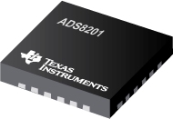

ADS8201是TI公司的一款精密ADC(<=10MSPS)产品,ADS8201是具有 PGA 和 SPI? 的 2.2V 至 5.5V、低功耗、12 位、100kSPS、8 通道 DAS,本页介绍了ADS8201的产品说明、应用、特性等,并给出了与ADS8201相关的TI元器件型号供参考。
ADS8201 - 具有 PGA 和 SPI? 的 2.2V 至 5.5V、低功耗、12 位、100kSPS、8 通道 DAS - 精密ADC(<=10MSPS) - 模数转换器 - TI公司(Texas Instruments,德州仪器)
The ADS8201 is a low-power, complete on-chip data acquisition system optimized for portable applications that require direct connections, wide dynamic range, and automatic operation with very low power consumption. The device includes a 12-bit, capacitor-based, successive approximation register (SAR) analog-to-digital converter (ADC); a high-performance, continuous-time programmable gain amplifier (PGA); and a fully automatic scan, 8-to-1 multiplexer (mux) with breakout to allow for system design flexibility.
Many other features are included to further optimize system operation. Conversion results may be saved in an onboard first-in/first-out (FIFO) buffer and read out at a later time. Each channel has a gain setting that can be loaded automatically when it is selected. To simplify the serial port design, the ADS8201 offers a high-speed, wide-voltage serial interface. The ADS8201 is ideal for sensor applications (for example, bridge sensors, pressure sensors, accelerometers, gyrosensors, temperature sensors, etc.) as used in gaming and navigation.
The ADS8201 is available in a 24-lead, 4×4 QFN package, and is specified over the –40°C to +85°C industrial temperature range.
- Low-Power, Flexible Supply Range:
- 2.2V to 5.5V Analog Supply
- 1.32mW (100kHz, +VA = 2.2V, +VD = 2.2V)
- 4.5mW (100kHz, +VA = 5V, +VD = 5V)
- Up to 100kSPS Throughput Rate
- Excellent DC Performance:
- ±0.5 LSB typ, ±1.5 LSB max INL
- ±0.5 LSB typ, ±1.0 LSB max DNL
- ±6 LSB Offset Error at +VA =5V
- ±0.1%FS Gain Error at +VA = 5V
- Flexible Analog Inputs:
- True Differential Input
- Differential/Unipolar Input Range (0 to VREF)
- TAG Bit Output
- Programmable Averaging Function
- Onboard, Eight Single-Ended/Four Differential Channel Mux:
- High Input Impedance
- High-Performance PGA (Gain = 1/2/4/8)
- PGA Breakout
- Auto/Manual Channel Select with Gain
- Auto/Manual Trigger
- Mixed Type Partial Scan
- Built-in Hardware Features:
- On-chip Conversion Clock (CCLK)
- Hardware/Software Reset
- Programmable Status/Polarity for BUSY/INT
- Flexible I/O:
- SPI-/DSP™-Compatible Serial Interface
- Separate I/O Supply (2.2V to 5.5V)
- Onboard 8×1 FIFO Buffer
- SCLK up to 25MHz (VD = 5V)
- Multi-Chip Ready and Fully Enabled:
- Global CONVST (Independent of CS)
- Power-Down Mode
- 24-Pin 4×4 QFN Package
- APPLICATIONS
- Portable Communications
- Transducer Interfaces
- Portable Medical Instruments
- Data Acquisition Systems
- GPS Chipsets
DSP is a trademark of Texas Instruments. SPI is a trademark of Motorola Inc. All other trademarks are the property of their respective owners


