



- BQ27542DRZT-G1 - 集成电路(IC) > 电源管理(PMIC) > 电池管理
- LMH1980MMEVAL/NOPB - 开发板,套件,编程器 > 评估板 > 评估和演示板及套件
- LDC1612EVM - 开发板,套件,编程器 > 评估板 > 传感器评估板
- LMK04806BISQE/NOPB - 集成电路(IC) > 时钟/定时 > 时钟发生器,PLL,频率合成器
- TLC074AIN - 集成电路(IC) > 线性 > 放大器 > 仪器,运算放大器,缓冲器
- ADC14C080CISQE/NOPB - 集成电路(IC) > 数据采集 > 模数转换器(ADC)
- MUX36S16IRTVR - 集成电路(IC) > 接口 > 模拟开关,多路复用器,解复用器
- LM22672MR-ADJ/NOPB - 集成电路(IC) > 电源管理(PMIC) > 稳压器 - DC-DC 开关稳压器
- SN74S139AN - 集成电路(IC) > 逻辑 > 信号开关,多路复用器,解码器
- LM3S5P51-IBZ80-C1T - 嵌入式 - 微控制器
- TRF3701EVM - 射频评估和开发套件,开发板
- 74ACT16374DLRG4 - 集成电路(IC) > 逻辑 > 触发器
- MSPM0G1107TRHBR - 集成电路(IC) > 嵌入式 > 微控制器
- LM2767M5X/NOPB - 集成电路(IC) > 电源管理(PMIC) > 稳压器 - DC-DC 开关稳压器
- SN74ALS03BDG4 - 逻辑 - 栅极和逆变器
- SN7407DR - 集成电路(IC) > 逻辑 > 缓冲器,驱动器,接收器,收发器
- ADS820U - 集成电路(IC) > 数据采集 > 模数转换器(ADC)
- PTH04T230WAS - 板安装电源 > 直流转换器
- CD74HC4002M - 集成电路(IC) > 逻辑 > 门和反相器
- J7200XSOMG01EVM - 开发板,套件,编程器 > 评估板 > 嵌入式 MCU、DSP 评估板



CD4098B - CMOS 双路单稳态多谐振荡器
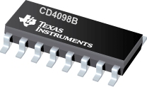
CD4098B是TI德州仪器公司的一款单稳多频振荡器产品,CD4098B是CMOS 双路单稳态多谐振荡器,本站介绍了CD4098B的封装应用图解、特点和优点、功能等,并给出了与CD4098B相关的TI元器件型号供参考。
CD4098B - CMOS 双路单稳态多谐振荡器 - 单稳多频振荡器 - 特殊逻辑 - 德州仪器
CD4098B dual monostable multivibrator provides stable retriggerable/resettable one-shot operation for any fixed-voltage timing application.
An external resistor (RX) and an external capacitor (CX) control the timing for the circuit. Adjustment of RX and CX provides a wide range of output pulse widths from the Q and Q\ terminals. The time delay from trigger input to output transition (trigger progagation delay) and the time delay from set input to output transition (reset progagation delay) are independent of RX and CX.
Leading-edge-triggering (+TR) and trailing-edge-triggering (-TR) input are provided for triggering from either edge of an input pulse. An unused +TR input should be tied to VSS. An unused (-TR) input should be tied to VDD. A RESET (on low level) is provided for immediate termination of the output pulse or to prevent output pulses when power is turned on. An unused RESET input should be tied to VDD. However, if an entire section of the CD4098B is not used, its RESET should be tied to VSS. See Table 1.
In normal operation the circuit triggers (extends the output pulse one period) on the application of each new trigger pulse. For operation in the non-retriggerable mode, Q\ is connected to -TR when leading-edge triggering (+TR) is used or Q is connected to +TR when trailing-edge triggering (-TR) is used.
The time period (T) for this multivibrator can be approximated by: TX= ½ RXCX for CX 0.01 uF. Time periods as a function of RX for values of CX and VDD are given in Fig. 8. Values of T vary from unit to unit and as a function of voltage, temperature, and RXCX.
The minimum value of external resistance, RX, is 5 k. The maximum value of external capacitance, CX, is 100uF. Fig.9 shows time periods as a function of CX for values of RX and VDD.
The output pulse width has variations of ±2.5% typically, over the temperature range of -55°C to 125°C for CX= 1000 pF and RX= 100 k.
For power supply variations of ±5%, the output pulse width has variations of ±0.5% typically, for VDD= 10 V and 15 V and ±1% typically, for VDD= 5 V at CX= 1000 pF and RX= 5 k.
These types are supplied in 16-lead hermetic dual-in-line ceramic packages (F3A suffix), 16-lead dual-in-line plastic package (E suffix), 16-lead small-outline packages (M, M96, and MT suffixes), and 16-lead thin shrink small-outline packages (PW and PWR suffixes).
The CD4098B is similar to type MC14528.
- Retriggerable/resettable capability
- Trigger and reset propagation delays independent of RX, CX
- Triggering from leading or trailing edge
- Q and Q\ buffered outputs available
- Separate resets
- Wide range of output-pulse widths
- 100% tested for maximum quiescent current at 20 V
- Maximum input current of 1 uA at 18 V over full package-temperature range; 100 nA at 18 V and 25°C
- Noise margin (full package-temperature range):
- 1 V at VDD = 5 V
- 2 V at VDD = 10 V
- 2.5 V at VDD = 15 V
- 5-V, 10-V, and 15-V parametric ratings
- Standardized, symmetrical output characteristics
- Meets all requirements of JEDEC Tentative Standard No. 13B, "Standard Specifications for Description of 'B' Series CMOS Devices."
- Applications:
- Pulse delay and timing
- Pulse shaping
- Astable multivibrator
- TPS77518 - 单输出 LDO、500mA、固定电压 (1.8V)、快速瞬态响应、SVS
- TPS3700 - 具有 18V 高电源(Vcc 时)的过压和欠压监控电路
- ADS6123 - 具有可选并行 CMOS 或 LVDS 输出的低功耗 12 位 80MSPS ADC
- DRV8806 - 四通道串行接口低侧驱动器 IC
- SN54ALS38B - 具有集电极开路输出的四路 2 输入正与非缓冲器
- TLV320AIC3254 - 采用可编程 miniDSP 的超低功耗立体声音频编解码器
- LM4906 - 具有内部可选增益的 1W、旁路电容器更少音频功率放大器
- TPS2147 - 用于 USB、DSP 和便携应用领域的 3.3V LDO + 双路开关,工作态低电平启用
- SN54ALS169B - 同步 4 位加/减二进制计数器
- UCD3020 - 具有多达 2 个稳压输出和 6 个 DPWM 输出的完全可编程的数字功率控制器

