



- UCC21759QDWQ1 - 隔离器 > 隔离器 - 栅极驱动器
- TPS71728DSET - 集成电路(IC) > 电源管理(PMIC) > 稳压器 - 线性
- CD74HC541PW - 集成电路(IC) > 逻辑 > 缓冲器,驱动器,接收器,收发器
- INA111BUG4 - 集成电路(IC) > 线性 > 放大器 > 仪器,运算放大器,缓冲器
- TPS628660AYCGR - 集成电路(IC) > 电源管理(PMIC) > 稳压器 - DC-DC 开关稳压器
- DS90CP02SPX/NOPB - 集成电路(IC) > 逻辑 > 信号开关,多路复用器,解码器
- AFE159RP4YAFR - 集成电路(IC) > 数据采集 > 模拟前端(AFE)
- LMH6553MRX/NOPB - 集成电路(IC) > 线性 > 放大器 > 仪器,运算放大器,缓冲器
- LP590722QDQNRQ1 - 集成电路(IC) > 电源管理(PMIC) > 稳压器 - 线性
- TRF7962ARHBT - 射频和无线 > RFID,射频接入,监控 IC
- DAC8043U/2K5 - 集成电路(IC) > 数据采集 > 数模转换器(DAC)
- OPA4343EA/250G4 - 集成电路(IC) > 线性 > 放大器 > 仪器,运算放大器,缓冲器
- 5962-8958701XA - 集成电路(IC) > 电源管理(PMIC) > 稳压器 - 线性稳压器控制器
- LM2595S-12 - 集成电路(IC) > 电源管理(PMIC) > 稳压器 - DC-DC 开关稳压器
- TPS65988DHRSHR - 集成电路(IC) > 电源管理(PMIC) > 电源管理 - 专用
- SN74F02D - 集成电路(IC) > 逻辑 > 门和反相器
- LM9036MX-5.0/NOPB - 集成电路(IC) > 电源管理(PMIC) > 稳压器 - 线性
- LM5085SD/NOPB - 集成电路(IC) > 电源管理(PMIC) > DC-DC 开关控制器
- SN74AHC123AMDREPG4 - 集成电路(IC) > 逻辑 > 多谐振荡器
- SN74CBT3244GQNR - 逻辑 - 信号开关,多路复用器,解码器



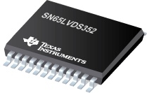
SN65LVDS352 - 具有 -4 至 5V 共模范围的四路 LVDS 接收器
SN65LVDS352是TI德州仪器公司的一款PECLPHY产品,SN65LVDS352是具有 -4 至 5V 共模范围的四路 LVDS 接收器,本站介绍了SN65LVDS352的封装应用图解、特点和优点、功能等,并给出了与SN65LVDS352相关的TI元器件型号供参考。
SN65LVDS352 - 具有 -4 至 5V 共模范围的四路 LVDS 接收器 - PECLPHY - LVDS/M-LVDS/ECL/CML - 德州仪器
The SN65LVDS348, SN65LVDT348, SN65LVDS352, and SN65LVDT352 are high-speed, quadruple differential receivers with a wide common-mode input voltage range. This allows receipt of TIA/EIA-644 signals with up to 3-V of ground noise or a variety of differential and single-ended logic levels. The ’348 is in a 16-pin package to match the industry-standard footprint of the DS90LV048. The ’352 adds two additional VCC and GND pins in a 24-pin package to provide higher data transfer rates with multiple receivers in operation. All offer a flow-through architecture with all inputs on one side and outputs on the other to ease board layout and reduce crosstalk between receivers. LVDT versions of both integrate a 110- line termination resistor.
These receivers also provide 3x the standard’s minimum common-mode noise voltage tolerance. The –4 V to 5 V common-mode range allows usage in harsh operating environments or accepts LVPECL, PECL, LVECL, ECL, CMOS, and LVCMOS levels without level shifting circuitry. See the Application Information Section for more details on the ECL/PECL to LVDS interface.
Precise control of the differential input voltage thresholds allows for inclusion of 50 mV of input-voltage hysteresis to improve noise rejection. The differential input thresholds are still no more than ±50 mV over the full input common-mode voltage range.
The receiver inputs can withstand ±15 kV human-body model (HBM), with respect to ground, without damage. This provides reliability in cabled and other connections where potentially damaging noise is always a threat.
The receivers also include a (patent-pending) failsafe circuit that provides a high-level output within 600 ns after loss of the input signal. The most common causes of signal loss are disconnected cables, shorted lines, or powered-down transmitters. This prevents noise from being received as valid data under these fault conditions. This feature may also be used for Wired-Or bus signaling.
The SN65LVDT348 and SN65LVDT352 include an integrated termination resistor. This reduces board space requirements and parts count by eliminating the need for a separate termination resistor. This can also improve signal integrity at the receiver by reducing the stub length from the line termination to the receiver.
The intended application of these devices and signaling technique is for point-to-point baseband data transmission over controlled impedance media of approximately 100 . The transmission media may be printed-circuit board traces, backplanes, or cables. The ultimate rate and distance of data transfer is dependent upon the attenuation characteristics of the media and the noise coupling to the environment.
The SN65LVDS348, SN65LVDT348, SN65LVDS352 and SN65LVDT352 are characterized for operation from –40°C to 85°C.
- Meets or Exceeds the Requirements of ANSI TIA/EIA-644A Standard
- Single-Channel Signaling Rates1 up to 560 Mbps
- –4 V to 5 V Common-Mode Input Voltage Range
- Flow-Through Architecture
- Active Failsafe Assures a High-level Output When an Input Signal Is not Present
- SN65LVDS348 Provides a Wide Common-Mode Range Replacement for the SN65LVDS048A or the DS90LV048A
- APPLICATIONS
- Logic Level Translator
- Point-to-Point Baseband Data Transmission Over 100- Media
- ECL/PECL-to-LVTTL Conversion
- Wireless Base Stations
- Central Office or PABX Switches
1The signaling rate of a line is the number of voltage transitions that are made per second expressed in the units bps (bits per second).
- TPS22968 - 双通道、超低电阻负载开关,TPS22968
- TPS3808-EP - 增强型产品低静态电流可编程延迟监控电路
- SN7447A - BCD 到 7 段解码器/驱动器
- DS90CR287 - +3.3V 上升沿数据选通 LVDS 28 位频道链接发送器 - 85 MHz
- TPS2224 - 具有串行接口且采用 24 引脚封装的 1A 双槽位 PC 卡电源开关
- LM235A - ±1°C 模拟输出温度传感器,军用级,采用气密性 TO 封装
- SN75ALS176 - 差动总线收发器
- SN74LVC1G3157 - 单极双闸模拟开关
- INA220B-Q1 - 具有两线制接口的高或者低侧、双向电流/功率监视器
- TPD7S019 - 用于 VGA 端口的 7 通道集成 ESD 解决方案,具有集成电平转换器和

