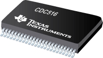

CDC516是TI公司的一款无产品,CDC516是具有三态输出的 3.3V 锁相环时钟驱动器,本页介绍了CDC516的产品说明、应用、特性等,并给出了与CDC516相关的TI元器件型号供参考。
CDC516 - 具有三态输出的 3.3V 锁相环时钟驱动器 - 无 - 零延迟缓冲器 - TI公司(Texas Instruments,德州仪器)
The CDC516 is a high-performance, low-skew, low-jitter, phase-lock loop clock driver. It uses a phase-lock loop (PLL) to precisely align, in both frequency and phase, the feedback output (FBOUT) to the clock (CLK) input signal. It is specifically designed for use with synchronous DRAMs. The CDC516 operates at 3.3-V VCC and is designed to drive up to five clock loads per output.
Four banks of four outputs provide 16 low-skew, low-jitter copies of the input clock. Output signal duty cycles are adjusted to 50 percent, independent of the duty cycle at the input clock. Each bank of outputs can be enabled or disabled separately via the 1G, 2G, 3G, and 4G control inputs. When the G inputs are high, the outputs switch in phase and frequency with CLK; when the G inputs are low, the outputs are disabled to the logic-low state.
Unlike many products containing PLLs, the CDC516 does not require external RC networks. The loop filter for the PLL is included on-chip, minimizing component count, board space, and cost.
Because it is based on PLL circuitry, the CDC516 requires a stabilization time to achieve phase lock of the feedback signal to the reference signal. This stabilization time is required following power up and application of a fixed-frequency, fixed-phase signal at CLK, as well as following any changes to the PLL reference or feedback signals. The PLL may be bypassed for test purposes by strapping AVCC to ground.
The CDC516 is characterized for operation from 0°C to 70°C.
- Use CDCVF2510A as a Replacement for this Device
- Phase-Lock Loop Clock Distribution for Synchronous DRAM Applications
- Distributes One Clock Input to Four Banks of Four Outputs
- Separate Output Enable for Each Output Bank
- External Feedback Pin (FBIN) Is Used to Synchronize the Outputs to the Clock Input
- No External RC Network Required
- Operates at 3.3-V VCC
- Packaged in Plastic 48-Pin Thin Shrink Small-Outline Package


