


- SN74ACT86PWE4 - 逻辑 - 栅极和逆变器
- CY74FCT162827CTPAC - 集成电路(IC) > 逻辑 > 缓冲器,驱动器,接收器,收发器
- M430FR5989SRGCREP - 集成电路(IC) > 嵌入式 > 微控制器
- SN74LVC2G04DBVT - 集成电路(IC) > 逻辑 > 门和反相器
- TS2DDR2811ZXYR - 集成电路(IC) > 接口 > 模拟开关,多路复用器,解复用器
- UCC27614QDSGRQ1 - 集成电路(IC) > 电源管理(PMIC) > 栅极驱动器
- TRS222IN - 集成电路(IC) > 接口 > 驱动器,接收器,收发器
- MSP430I2020TPWR - 集成电路(IC) > 嵌入式 > 微控制器
- ADS7958SDBTR - 集成电路(IC) > 数据采集 > 模数转换器(ADC)
- DS26C32ATM/NOPB - 集成电路(IC) > 接口 > 驱动器,接收器,收发器
- LM27961TL/NOPB - 集成电路(IC) > 电源管理(PMIC) > LED 驱动器
- AM26C31IPWR - 集成电路(IC) > 接口 > 驱动器,接收器,收发器
- LM2940CS-12 - 集成电路(IC) > 电源管理(PMIC) > 稳压器 - 线性
- LM48861TM/NOPB - 集成电路(IC) > 线性 > 放大器 > 音频放大器
- TMP451JQDQFTQ1 - 传感器,变送器 > 温度传感器 > 模拟和数字输出
- TMS320C6455BGTZ2 - 集成电路(IC) > 嵌入式 > DSP(数字信号处理器)
- TLC5929RGER - 集成电路(IC) > 电源管理(PMIC) > LED 驱动器
- UA78L05ACLP - 集成电路(IC) > 电源管理(PMIC) > 稳压器 - 线性
- SNJ54LS375J - 集成电路(IC) > 逻辑 > 锁存器
- ISO7420MDR - 隔离器 > 数字隔离器


CDCL1810 - 1.8V Ten Outputs High Performance Clock Distributor
CDCL1810是TI德州仪器公司的一款分频器产品,CDCL1810是1.8V Ten Outputs High Performance Clock Distributor,本站介绍了CDCL1810的封装应用图解、特点和优点、功能等,并给出了与CDCL1810相关的TI元器件型号供参考。
CDCL1810 - 1.8V Ten Outputs High Performance Clock Distributor - 分频器 - 时钟缓冲器 - 德州仪器
- Single 1.8-V Supply
- High-Performance Clock Distributor with 10 Outputs
- Low Input-to-Output Additive Jitter: as Low as 10fs RMS
- Output Group Phase Adjustment
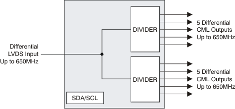
- Low-Voltage Differential Signaling (LVDS) Input, 100-Ω Differential On-Chip Termination, up to 650 MHz Frequency
- Differential Current Mode Logic (CML) Outputs, 50-Ω Single-Ended On-Chip Termination, up to 650 MHz Frequency
- Two Groups of Five Outputs Each with Independent Frequency Division Ratios
- Output Frequency Derived with Divide Ratios of 1, 2, 4, 5, 8, 10, 16, 20, 32, 40, and 80
- Meets ANSI TIA/EIA-644-A-2001 LVDS Standard Requirements
- Power Consumption: 410 mW Typical
- Output Enable Control for Each Output and Automatic Output Synchronization
- SDA/SCL Device Management Interface
- 48-pin VQFN (RGZ) Package
- Industrial Temperature Range: –40°C to +85°C
- Distribution for High-Speed SERDES
- Distribution of SERDES Reference Clocks for 1G/10G Ethernet, 1X/2X/4X/10X Fibre Channel, PCI Express, Serial ATA, SONET, CPRI, OBSAI, etc.
- Up to 1-to-10 Clock Buffering and Fan-out
The CDCL1810 is a high-performance clock distributor. The programmable dividers, P0 and P1, give a high flexibility to the ratio of the output frequency to the input frequency: FOUT = FIN/P, where: P (P0,P1) = 1, 2, 4, 5, 8, 10, 16, 20, 32, 40, 80.
The CDCL1810 supports one differential LVDS clock input and a total of 10 differential CML outputs. The CML outputs are compatible with LVDS receivers if they are ac-coupled.
With careful observation of the input voltage swing and common-mode voltage limits, the CDCL1810 can support a single-ended clock input as outlined in Pin Configuration and Functions.
All device settings are programmable through the SDA/SCL, serial two-wire interface. The serial interface is 1.8V tolerant only.
The phase of one output group relative to the other can be adjusted through the SDA/SCL interface. For post-divide ratios (P0, P1) that are multiples of 5, the total number of phase adjustment steps (n) equals the divide-ratio divided by 5. For post-divide ratios (P0, P1) that are not multiples of 5, the total number of steps (n) is the same as the post-divide ratio. The phase adjustment step (ΔΦ) in time units is given as: ΔΦ = 1/(n × FOUT), where FOUT is the respective output frequency.
The device operates in a 1.8-V supply environment and is characterized for operation from –40°C to +85°C. The CDCL1810 is available in a 48-pin VQFN (RGZ) package.
| PART NUMBER | PACKAGE | BODY SIZE (NOM) |
|---|---|---|
| CDCL1810 | VQFN (48) | 7.00 mm × 7.00 mm |
- PTN78000A - 1.5 A、宽输入、非隔离、宽负输出调节模块
- SN74GTL16622A - 18 位 LVTTL 到 GTL/GTL+ 总线收发器
- DCP012415DB - 微型 1W 隔离未稳压 DC/DC 转换器
- TRS222 - 具有 +/-15kV ESD 保护的 5V 双路 RS-232 线路驱动器/接收器
- UCC3837 - 8 引脚 N-FET 线性稳压器控制器
- TPA3118D2 - 30W 无滤波器 D 类立体声放大器,带 AM 抑制
- TPA3144D2 - 低成本 10W 无电感立体声 (BTL) D 类音频放大器
- SN74LVC1G14 - 单路施密特触发反向器
- ADS62P23 - 具有可选 DDR LVDS 或 CMOS 输出的双路 12 位 80MSPS ADC
- TM4C129DNCZAD - Tiva C 系列微控制器

