


- SNJ54F36J - 集成电路(IC) > 逻辑 > 门和反相器
- OPA2171AIDR - 集成电路(IC) > 线性 > 放大器 > 仪器,运算放大器,缓冲器
- SN74AHC125QDRG4 - 集成电路(IC) > 逻辑 > 缓冲器,驱动器,接收器,收发器
- TPS73618DBVT - 集成电路(IC) > 电源管理(PMIC) > 稳压器 - 线性
- TLV70733APDQNR - 集成电路(IC) > 电源管理(PMIC) > 稳压器 - 线性
- CDC3S04EVM - 开发板,套件,编程器 > 评估板 > 评估和演示板及套件
- SN74AVC1T45DCKRG4 - 集成电路(IC) > 逻辑 > 转换器,电平移位器
- CY74FCT257CTD - 集成电路(IC) > 逻辑 > 信号开关,多路复用器,解码器
- TPS3613-01DGSG4 - 集成电路(IC) > 电源管理(PMIC) > 监控器
- TPS563219ADDFT - 集成电路(IC) > 电源管理(PMIC) > 稳压器 - DC-DC 开关稳压器
- 74AC11000N - 集成电路(IC) > 逻辑 > 门和反相器
- TPS54240DGQ - 集成电路(IC) > 电源管理(PMIC) > 稳压器 - DC-DC 开关稳压器
- LMV7235M7 - 集成电路(IC) > 线性 > 比较器
- DS92LV1023TMSA/NOPB - 集成电路(IC) > 接口 > 串行器,解串器
- LM3S6918-IBZ50-A2 - 集成电路(IC) > 嵌入式 > 微控制器
- LMC7211AIM/NOPB - 集成电路(IC) > 线性 > 比较器
- TPS73133MDBVREP - 集成电路(IC) > 电源管理(PMIC) > 稳压器 - 线性
- LM3S1621-IBZ80-C5 - 嵌入式 - 微控制器
- LM3S5G31-IBZ80-A2 - 嵌入式 - 微控制器
- TRS202EIPWRG4 - 集成电路(IC) > 接口 > 驱动器,接收器,收发器


CDCLVP1102 - 低抖动 1:2 通用 LVPECL 缓冲器
CDCLVP1102是TI德州仪器公司的一款差动产品,CDCLVP1102是低抖动 1:2 通用 LVPECL 缓冲器,本站介绍了CDCLVP1102的封装应用图解、特点和优点、功能等,并给出了与CDCLVP1102相关的TI元器件型号供参考。
CDCLVP1102 - 低抖动 1:2 通用 LVPECL 缓冲器 - 差动 - 时钟缓冲器 - 德州仪器
- 1:2 Differential Buffer
- Single Clock Input
- Universal Inputs Can Accept LVPECL, LVDS, LVCMOS/LVTTL
- Two LVPECL Outputs
- Maximum Clock Frequency: 2 GHz
- Maximum Core Current Consumption: 33 mA
- Very Low Additive Jitter: <100 fs, RMS in 10-kHz to 20-MHz Offset Range
- 2.375-V to 3.6-V Device Power Supply
- Maximum Propagation Delay: 450 ps
- Maximum Output Skew: 10 ps
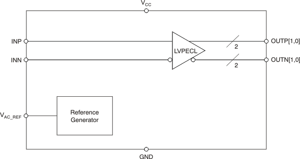
- LVPECL Reference Voltage, VAC_REF, Available for Capacitive-Coupled Inputs
- Industrial Temperature Range: –40°C to 85°C
- Supports 105°C PCB Temperature (Measured at Thermal Pad)
- Available in 3-mm × 3-mm QFN-16 (RGT) Package
- ESD Protection Exceeds 2 kV (HBM)
- Wireless Communications
- Telecommunications/Networking
- Medical Imaging
- Test and Measurement Equipment
The CDCLVP1102 is a highly versatile, low additive jitter buffer that can generate two copies of LVPECL clock outputs from one LVPECL, LVDS, or LVCMOS input for a variety of communication applications. It has a maximum clock frequency up to 2 GHz. The overall additive jitter performance is less than 0.1 ps, RMS from 10 kHz to 20 MHz, and overall output skew is as low as 10 ps, making the device a perfect choice for use in demanding applications.
The CDCLVP1102 clock buffer distributes a single clock input (IN) to two pairs of differential LVPECL clock outputs (OUT0, OUT1) with minimum skew for clock distribution. The inputs can be LVPECL, LVDS, or LVCMOS/LVTTL.
The CDCLVP1102 is specifically designed for driving 50-Ω transmission lines. When driving the inputs in single-ended mode, the LVPECL bias voltage (VAC_REF) should be applied to the unused negative input pin. However, for high-speed performance up to 2 GHz, differential mode is strongly recommended.
The CDCLVP1102 is characterized for operation from –40°C to 85°C and is available in a QFN-16, 3-mm × 3-mm package.
| PART NUMBER | PACKAGE | BODY SIZE (NOM) |
|---|---|---|
| CDCLVP1102 | QFN (16) | 3.00 mm × 3.00 mm |
- TLV1548-Q1 - 具有串行控制和 8 个模拟输入的汽车类低压 10 位模数转换器
- MSP430FG479 - 16 位超低功耗 MCU、60KB Flash、2KB RAM、16 位 Sigma-Delta ADC、12 位 DAC、运算放大器、128Seg LCD
- TPS63011 - 具有 2A 开关的高效率、单电感器、降压升压转换器
- LM3754 - 具有集成 FET 驱动器和线性稳压器控制器的可扩展 2 相同步降压控制器
- BQ32000 - Serial RTC
- TPS60151 - 采用 2x2 QFN 封装的 140mA、5V 充电泵
- TMS320F2806 - 具有闪存的 32 位数字信号控制器
- SN74LVC374A-Q1 - 汽车类具有三态输出的八路边沿 D 类触发器
- DP83630 - 精密 PHYTER - IEEE 1588 精确时间协议收发器
- LP3919 - CDMA Cellular Phone Power Management Unit

