



- UCC3974PW - 集成电路(IC) > 电源管理(PMIC) > 照明,镇流器控制器
- ISO3082DWRG4 - 集成电路(IC) > 接口 > 驱动器,接收器,收发器
- SN74AHCT139DBR - 集成电路(IC) > 逻辑 > 信号开关,多路复用器,解码器
- TLC2252ID - 集成电路(IC) > 线性 > 放大器 > 仪器,运算放大器,缓冲器
- TPS2813P - 集成电路(IC) > 电源管理(PMIC) > 栅极驱动器
- INA190A2QDDFRQ1 - 集成电路(IC) > 线性 > 放大器 > 仪器,运算放大器,缓冲器
- LP3988QMFX-2P85 - 集成电路(IC) > 电源管理(PMIC) > 稳压器 - 线性
- MSP430FR2032IG56 - 集成电路(IC) > 嵌入式 > 微控制器
- MSP430F2112TRTVR - 集成电路(IC) > 嵌入式 > 微控制器
- TLV9022DR - 集成电路(IC) > 线性 > 比较器
- SN74ALS299NSRE4 - 逻辑 - 移位寄存器
- JM38510/30906SEA - 集成电路(IC) > 逻辑 > 信号开关,多路复用器,解码器
- CC2400-RTB1 - 射频和无线 > 射频收发器 IC
- LM393ADR - 集成电路(IC) > 线性 > 比较器
- TAA5242IRGER - 集成电路(IC) > 数据采集 > ADC/DAC - 特殊用途
- SN74ABT162601DLR - 集成电路(IC) > 逻辑 > 通用总线功能
- TLC1551IFN - 集成电路(IC) > 数据采集 > 模数转换器(ADC)
- MSP430F5435IPNR - 集成电路(IC) > 嵌入式 > 微控制器
- CC430F6126IRGC - 射频和无线 > 射频收发器 IC
- CC2510F8RSPR - 射频和无线 > 射频收发器 IC



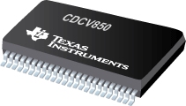
CDCV850 - 2.5V 锁相环差动时钟驱动器,具有 2 线路串行接口
CDCV850是TI德州仪器公司的一款无产品,CDCV850是2.5V 锁相环差动时钟驱动器,具有 2 线路串行接口,本站介绍了CDCV850的封装应用图解、特点和优点、功能等,并给出了与CDCV850相关的TI元器件型号供参考。
CDCV850 - 2.5V 锁相环差动时钟驱动器,具有 2 线路串行接口 - 无 - 零延迟缓冲器 - 德州仪器
The CDCV850 is a high-performance, low-skew, low-jitter zero delay buffer that distributes a differential clock input pair (CLK, CLK) to ten differential pairs of clock outputs (Y[0:9], Y[0:9]) and one differential pair of feedback clock outputs (FBOUT, FBOUT). The clock outputs are controlled by the clock inputs (CLK, CLK), the feedback clocks (FBIN, FBIN), the 2-line serial interface (SDATA,SCLK), and the analog power input (AVDD). A two-line serial interface can put the individual output clock pairs in a high-impedance state. When the AVDD terminal is tied to GND, the PLL is turned off and bypassed for test purposes.
The device provides a standard mode (100 Kbits/s) 2-line serial interface for device control. The implementation is as a slave/receiver. The device address is specified in the 2-line serial device address table. Both of the 2-line serial inputs (SDATA and SCLK) provide integrated pullup resistors (typically 100 kΩ).
Two 8-bit, 2-line serial registers provide individual enable control for each output pair. All outputs default to enabled at powerup. Each output pair can be placed in a high-impedance mode, when a low-level control bit is written to the control register. The registers must be accessed in sequential order (i.e., random access of the registers not supported). The serial interface circuit can be supplied with either 2.5 V or 3.3 V (at VDDI) in applications where this programming option is not required (after power up, all output pairs will then be enabled).
When the input frequency falls below a suggested detection frequency that is below 20 MHz (typically 10 MHz), the output pairs are put into a high-impedance condition, the PLL is shut down, and the device will enter a low power mode. The CDCV850 is also able to track spread spectrum clocking for reduced EMI.
Since the CDCV850 is based on PLL circuitry, it requires a stabilization time to achieve phase-lock of the PLL. This stabilization time is required following power up, as well as changes to various 2-line serial registers that affect the PLL. The CDCV850 is characterized in a temperature range from –40°C to 85°C.
- Phase-Lock Loop Clock Driver for Double Data-Rate Synchronous DRAM Applications
- Spread Spectrum Clock Compatible
- Operating Frequency: 60 to 140 MHz
- Low Jitter (cyc.cyc): ±75 ps
- Distributes One Differential Clock Input to Ten Differential Outputs
- Two-Line Serial Interface Provides Output Enable and Functional Control
- Outputs Are Put Into a High-Impedance State When the Input Differential Clocks Are <20 MHz
- 48-Pin TSSOP Package
- Consumes <250-µA Quiescent Current
- External Feedback Pins (FBIN, FBIN) Are Used to Synchronize the Outputs to the Input Clocks
- LM62 - ±2°C 模拟输出温度传感器
- OPT9221 - OPT9221 飞行时间控制器
- DCP021212D - 微型 2W 隔离未稳压 DC/DC 转换器
- TPS630252 - 采用 WCSP 封装的 4A 开关单电感降压/升压转换器
- TPS3125J18 - 采用 5/SOT23 封装且具有 /MR 的单通道 (1.8V) SVS
- DS481 - 具有休眠模式的低功耗 RS-485/RS-422 多点收发器
- TSU8111 - 具有双集成 USB2.0 开关和配件检测功能的单节 USB 充电器
- ADS1174 - 四路 16 位同步采样模数转换器
- SN54AS08 - 四路 2 输入正与门
- SN54AS175B - 具有清零功能的六路/四路 D 类触发器

