



- SN74F163ANSR - 集成电路(IC) > 逻辑 > 计数器,除法器
- LM2903P - 集成电路(IC) > 线性 > 比较器
- TPSM8F7420APG - 板安装电源 > 直流转换器
- SN74LVC2G74DCTRE6 - 集成电路(IC) > 逻辑 > 触发器
- SN74AUP1G08DBVT - 集成电路(IC) > 逻辑 > 门和反相器
- SN65LVDT14PWG4 - 集成电路(IC) > 接口 > 驱动器,接收器,收发器
- LP-XDS110 - 开发板,套件,编程器 > 编程器、仿真器和调试器
- LM5068MMX-2 - 集成电路(IC) > 电源管理(PMIC) > 热插拔控制器
- TPS65290LMRHFT - 集成电路(IC) > 电源管理(PMIC) > 特殊用途稳压器
- LM4040DEM3-5.0 - 集成电路(IC) > 电源管理(PMIC) > 电压基准
- LM239PWRE4 - 集成电路(IC) > 线性 > 比较器
- CC2630F128RSMR - 射频和无线 > 射频收发器 IC
- MAX232ECPWR - 集成电路(IC) > 接口 > 驱动器,接收器,收发器
- INA201AIDGKTG4 - 集成电路(IC) > 电源管理(PMIC) > 电流调节/管理
- SN74LVCR16245ADGG - 集成电路(IC) > 逻辑 > 缓冲器,驱动器,接收器,收发器
- LM2736Y EVAL/NOPB - 开发板,套件,编程器 > 评估板 > DC/DC 和 AC/DC(离线)SMPS 评估板
- TPS7A1650DRBT - 集成电路(IC) > 电源管理(PMIC) > 稳压器 - 线性
- TPS62875QWRZVRQ1 - 集成电路(IC) > 电源管理(PMIC) > 稳压器 - DC-DC 开关稳压器
- CSD18532NQ5B - 分立半导体产品 > 晶体管 > FET,MOSFET > 单 FET,MOSFET
- TMP1075EVM - 开发板,套件,编程器 > 评估板 > 传感器评估板



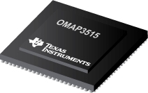
OMAP3515 - 应用处理器
OMAP3515是TI德州仪器公司的一款ARMCortex-A8产品,OMAP3515是应用处理器,本站介绍了OMAP3515的封装应用图解、特点和优点、功能等,并给出了与OMAP3515相关的TI元器件型号供参考。
OMAP3515 - 应用处理器 - ARMCortex-A8 - Sitara处理器 - 德州仪器
devices are based on the enhanced OMAP 3 architecture.
The OMAP 3 architecture is designed to provide best-in-class video, image, and graphics processing sufficient to support the following:
Streaming video Video conferencing High-resolution still imageThe device supports high-level operating systems (HLOSs), such as:
Linux® Windows® CE Android™This OMAP device includes state-of-the-art power-management techniques required for high-performance mobile products.
The following subsystems are part of the device:
Microprocessor unit (MPU) subsystem based on the ARM Cortex-A8 microprocessor PowerVR SGX subsystem for 3D graphics acceleration to support display (OMAP35 device only) Camera image signal processor (ISP) that supports multiple formats and interfacing options connected to a wide variety of image sensors Display subsystem with a wide variety of features for multiple concurrent image manipulation, and a programmable interface supporting a wide variety of displays. The display subsystem also supports NTSC and PAL video out. Level 3 (L3) and level 4 (L4) interconnects that provide high-bandwidth data transfers for multiple initiators to the internal and external memory controllers and to on-chip peripheralsThe device also offers:
A comprehensive power- and clock-management scheme that enables high-performance, low-power operation, and ultralow-power standby features. The device also supports SmartReflex adaptative voltage control. This power-management technique for automatic control of the operating voltage of a module reduces the active power consumption. Memory-stacking feature using the package-on-package (POP) implementation (CBB and CBC packages only)OMAP35 devices are available in a 515-pin s-PBGA package (CBB suffix), 515-pin s-PBGA package (CBC suffix), and a 423-pin s-PBGA package (CUS suffix). Some features of the CBB and CBC packages are not available in the CUS package. (See Table 1-1 for package differences).
This data manual presents the electrical and mechanical specifications for the OMAP35 applications processors. The information in this data manual applies to both the commercial and extended temperature versions of the OMAP35 applications processors unless otherwise indicated. This data manual consists of the following sections:
Section 2: Terminal Description: assignment, electrical characteristics, multiplexing, and functional description Section 3: Electrical Characteristics: power domains, operating conditions, power consumption, and DC characteristics Section 4: Clock Specifications input and output clocks, DPLL and DLL Section 5: Video Dac Specifications Section 6: Timing Requirements and Switching Characteristics Section 7: Package Characteristics: thermal characteristics, device nomenclature, and mechanical data for available packaging
- OMAP3 Devices:
- OMAP™ 3 Architecture
- MPU Subsystem
- Up to 720-MHz ARM® Cortex™-A8 Core
- NEON™ SIMD Coprocessor
- PowerVR® SGX™ Graphics Accelerator
- Tile-Based Architecture Delivering up to 1 MPoly/sec
- Universal Scalable Shader Engine: Multi-threaded Engine Incorporating Pixel and Vertex Shader Functionality
- Industry Standard API Support: OpenGLES 1.1 and 2.0, OpenVG1.0
- Fine-Grained Task Switching, Load Balancing, and Power Management
- Programmable High-Quality Image Anti-Aliasing
- Fully Software-Compatible with ARM9™
- Commercial and Extended Temperature Grades
- ARM Cortex-A8 Core
- ARMv7 Architecture
- TrustZone®
- Thumb®-2
- MMU Enhancements
- In-Order, Dual-Issue, Superscalar Microprocessor Core
- NEON Multimedia Architecture
- Over 2x Performance of ARMv6 SIMD
- Supports Both Integer and Floating-Point SIMD
- Jazelle® RCT Execution Environment Architecture
- Dynamic Branch Prediction with Branch Target Address Cache, Global History Buffer, and 8-Entry Return Stack
- Embedded Trace Macrocell (ETM) Support for Noninvasive Debug
- ARMv7 Architecture
- ARM Cortex-A8 Memory Architecture:
- -KB Instruction Cache (4-Way Set-Associative)
- -KB Data Cache (4-Way Set-Associative)
- -KB L2 Cache
- 112KB of ROM
- 64KB of Shared SRAM
- Endianess:
- ARM Instructions – Little Endian
- ARM Data – Configurable
- External Memory Interfaces:
- General Purpose Memory Controller (GPMC)
- 16-Bit-Wide Multiplexed Address and Data Bus
- Up to 8 Chip-Select Pins with 128-MB Address Space per Chip-Select Pin
- Glueless Interface to NOR Flash, NAND Flash (with ECC Hamming Code Calculation), SRAM, and Pseudo-SRAM
- Flexible Asynchronous Protocol Control for Interface to Custom Logic (FPGA, CPLD, ASICs, and so forth)
- Nonmultiplexed Address and Data Mode (Limited 2-KB Address Space)
- General Purpose Memory Controller (GPMC)
- System Direct Memory Access (sDMA) Controller (32 Logical Channels with Configurable Priority)
- Camera Image Signal Processor (ISP)
- CCD and CMOS Imager Interface
- Memory Data Input
- BT.601 (8-Bit) and BT.656 (10-Bit) Digital YCbCr 4:2:2 Interface
- Glueless Interface to Common Video Decoders
- Resize Engine
- Resize Images From 1/4x to 4x
- Separate Horizontal and Vertical Control
- Display Subsystem
- Parallel Digital Output
- Up to 24-Bit RGB
- HD Maximum Resolution
- Supports Up to 2 LCD Panels
- Support for Remote Frame Buffer Interface (RFBI) LCD Panels
- 2 10-Bit Digital-to-Analog Converters (DACs) Supporting:
- Composite NTSC and PAL Video
- Luma and Chroma Separate Video (S-Video)
- Rotation 90-, 180-, and 270-Degrees
- Resize Images From 1/4x to 8x
- Color Space Converter
- 8-Bit Alpha Blending
- Parallel Digital Output
- Serial Communication
- 5 Multichannel Buffered Serial Ports (McBSPs)
- 512-Byte Transmit and Receive Buffer (McBSP1, McBSP3, McBSP4, and McBSP5)
- 5-KB Transmit and Receive Buffer (McBSP2)
- SIDETONE Core Support (McBSP2 and McBSP3 Only) For Filter, Gain, and Mix Operations
- Direct Interface to I2S and PCM Device and TDM Buses
- 128-Channel Transmit and Receive Mode
- Four Master or Slave Multichannel Serial Port Interface (McSPI) Ports
- High-, Full-, and Low-Speed USB OTG Subsystem (12- and 8-Pin ULPI Interface)
- High-, Full-, and Low-Speed Multiport USB Host Subsystem
- 12- and 8-Pin ULPI Interface or 6-, 4-, and 3-Pin Serial Interface
- One HDQ™/1-Wire® Interface
- UARTs (One with Infrared Data Association [IrDA] and Consumer Infrared [CIR] Modes)
- Three Master and Slave High-Speed Inter-Integrated Circuit (I2C) Controllers
- 5 Multichannel Buffered Serial Ports (McBSPs)
- Removable Media Interfaces:
- Three Multimedia Card (MMC)/Secure Digital (SD) with Secure Data I/O (SDIO)
- Comprehensive Power, Reset, and Clock Management
- SmartReflex™ Technology
- Dynamic Voltage and Frequency Scaling (DVFS)
- Test Interfaces
- IEEE 1149.1 (JTAG) Boundary-Scan Compatible
- ETM Interface
- Serial Data Transport Interface (SDTI)
- 12 32-Bit General-Purpose Timers
- 2 32-Bit Watchdog Timers
- 1 32-Bit 32-kHz Sync Timer
- Up to General-Purpose I/O (GPIO) Pins (Multiplexed with Other Device Functions)
- 5-nm CMOS Technologies
- Package-On-Package (POP) Implementation for Memory Stacking (Not Available in CUS Package)
- Discrete Memory Interface
- Packages:
- 1.8-V I/O and 3.0-V (MMC1 Only), Note: These are default Operating Performance Point (OPP) voltages and could be optimized to lower values using SmartReflex AVS.
- TL750M05 - 单输出 LDO、750mA、固定电压 (5.0V)、低静态电流、60V 负载突降保护
- BQ2201 - SRAM 非易失性控制器 IC,用于 1 个 SRAM 内存组
- LP3985 - 微功耗,150mA 低噪声超低压降 CMOS 电压稳压器
- SN74ABTH16823 - 具有三态输出的 18 位总线接口触发器
- TPS2056A - 0.345A 2.7-5.5V 双路(1 输入/2 输出)高侧 MOSFET,具有故障报告和工作态高电平启用功能
- MSP430I2020 - MSP430i2040 混合信号微控制器
- CD74HC7266 - 高速 CMOS 逻辑四路 2 输入异或非门
- LM5115 - 75V、次级侧后置稳压器/同步降压控制器
- TRS202 - 具有 +/-15kV ESD 保护的 5V 双路 RS-232 线路驱动器/接收器
- LMV232 - 用于 CDMA 和 WCDMA 的双通道集成均方根功率检测器

