



- TLVH431AIDBZTG4 - 集成电路(IC) > 电源管理(PMIC) > 电压基准
- TPS2413DR - 集成电路(IC) > 电源管理(PMIC) > OR 控制器,理想二极管
- TLC3574IDWRG4 - 集成电路(IC) > 数据采集 > 模数转换器(ADC)
- CD74AC175NSR - 集成电路(IC) > 逻辑 > 触发器
- F28P650DK8NMRR - 集成电路(IC) > 嵌入式 > 微控制器
- AMC1304L25DW - 集成电路(IC) > 数据采集 > ADC/DAC - 特殊用途
- LM5177DCPR - 集成电路(IC) > 电源管理(PMIC) > DC-DC 开关控制器
- TPS75801KTTR - 集成电路(IC) > 电源管理(PMIC) > 稳压器 - 线性
- CD4521BE - 集成电路(IC) > 逻辑 > 计数器,除法器
- TMS320F28378DPTPS - 集成电路(IC) > 嵌入式 > 微控制器
- TL343IDBVR - 集成电路(IC) > 线性 > 放大器 > 仪器,运算放大器,缓冲器
- INA293B3QDBVRQ1 - 集成电路(IC) > 线性 > 放大器 > 仪器,运算放大器,缓冲器
- LMV821DBVR - 集成电路(IC) > 线性 > 放大器 > 仪器,运算放大器,缓冲器
- LM2832ZSDX - 集成电路(IC) > 电源管理(PMIC) > 稳压器 - DC-DC 开关稳压器
- TMS320DM335DZCE216 - 集成电路(IC) > 嵌入式 > DSP(数字信号处理器)
- BQ2060ADBQR - 集成电路(IC) > 电源管理(PMIC) > 电池管理
- SN2903QDGKRQ1 - 未分类 > 未分类
- TLV320AIC12IDBT - 集成电路(IC) > 接口 > 编解码器
- TMP123AIDBVR - 传感器,变送器 > 温度传感器 > 模拟和数字输出
- SN74LV00ARGYR - 集成电路(IC) > 逻辑 > 门和反相器



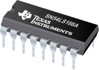
SN54LS166A - 并联负载 8 位移位寄存器
SN54LS166A是TI德州仪器公司的一款移位寄存器产品,SN54LS166A是并联负载 8 位移位寄存器,本站介绍了SN54LS166A的封装应用图解、特点和优点、功能等,并给出了与SN54LS166A相关的TI元器件型号供参考。
SN54LS166A - 并联负载 8 位移位寄存器 - 移位寄存器 - 触发器/锁存器/寄存器 - 德州仪器
The '166 and 'LS166A 8-bit shift registers are compatible with most other TTL logic families. All '166 and 'LS166A inputs are buffered to lower the drive requirements to one Series 54/74 or Series 54LS/74LS standard load, respectively. Input clamping diodes minimize switching transients and simplify system design.
These parallel-in or serial-in, serial-out shift registers have a complexity of 77 equivalent gates on a monolithic chip. They feature gated clock inputs and an overriding clear input. The parallel-in or serial-in modes are established by the shift/load input. When high, this input enables the serial data input and couples the eight flip-flops for serial shifting with each clock pulse. When low, the parallel (broadside) data inputs are enabled and synchronous loading occurs on the next clock pulse. During parallel loading, serial data flow is inhibited. Clocking is accomplished on the low-to-high-level edge of the clock pulse through a two-input positive NOR gate permitting one input to be used as a clock-enable or clock-inhibit function. Holding either of the clock inputs high inhibits clocking; holding either low enables the other clock input. This, of course, allows the system clock to be free-running and the register can be stopped on command with the other clock input. The clock inhibit input should be changed to the high level only while the clock input is high. A buffered, direct clear input overrides all other inputs, including the clock, and sets all flip-flops to zero.
- Synchronous Load
- Direct Overriding Clear
- Parallel to Serial Conversion
- VSP5611 - 16 位 50MSPS 4 通道成像模拟前端
- AFE5805 - 用于超声波的 8 通道模拟前端
- SN54ACT8990 - 测试总线控制器
- TPS767D318 - 双路输出低压降 (LDO) 稳压器
- SN54LS32 - 四路 2 输入正或门
- UCC2895 - BiCMOS 高级相移谐振控制器
- LM810 - 3 引脚微处理器重置电路
- TPA2026D2 - 具有动态范围的 3.2W/通道立体声 SmartGainTM D 类音频放大器
- BQ24620 - 用于磷酸锂电池的 28V 同步开关模式充电管理 IC
- SN74ALS561A - 具有三态输出的同步 4 位二进制计数器

