



- TLE2082CP - 集成电路(IC) > 线性 > 放大器 > 仪器,运算放大器,缓冲器
- SN75LVDS86ADGGR - 集成电路(IC) > 接口 > 驱动器,接收器,收发器
- SN74ABT3611-20PCB - 集成电路(IC) > 逻辑 > FIFO 存储器
- TPSM831022SIUR - 板安装电源 > 直流转换器
- LP2985ITP-1.8/NOPB - 电源管理IC - 稳压器 - 线性
- CD74ACT14M - 集成电路(IC) > 逻辑 > 门和反相器
- TMCS1123C2AQDVGR - 传感器,变送器 > 电流传感器
- LM3202TL/NOPB - 集成电路(IC) > 电源管理(PMIC) > 稳压器 - DC-DC 开关稳压器
- SN74AHCT541PWRG3 - 集成电路(IC) > 逻辑 > 缓冲器,驱动器,接收器,收发器
- LM98714EB01/NOPB - 开发板,套件,编程器 > 评估板 > 评估和演示板及套件
- TS3V340D - 集成电路(IC) > 接口 > 模拟开关 - 特殊用途
- LM2937IMP-8.0 - 集成电路(IC) > 电源管理(PMIC) > 稳压器 - 线性
- SNJ54LS241FK - 集成电路(IC) > 逻辑 > 缓冲器,驱动器,接收器,收发器
- TLC274IPWRG4 - 集成电路(IC) > 线性 > 放大器 > 仪器,运算放大器,缓冲器
- LP38692MPX-5.0 - 集成电路(IC) > 电源管理(PMIC) > 稳压器 - 线性
- SN74AHCT374PW - 集成电路(IC) > 逻辑 > 触发器
- DUAL-DIYAMP-EVM - 开发板,套件,编程器 > 评估板 > 运算放大器评估板
- SN74LV4046APWR - 集成电路(IC) > 时钟/定时 > 时钟发生器,PLL,频率合成器
- TMS320C5515AZCH12 - 集成电路(IC) > 嵌入式 > DSP(数字信号处理器)
- LM4876MM/NOPB - 集成电路(IC) > 线性 > 放大器 > 音频放大器



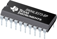
SN54LS373-SP - 具有三态输出的八路 D 类透明锁存器
SN54LS373-SP是TI德州仪器公司的一款D类锁存器产品,SN54LS373-SP是具有三态输出的八路 D 类透明锁存器,本站介绍了SN54LS373-SP的封装应用图解、特点和优点、功能等,并给出了与SN54LS373-SP相关的TI元器件型号供参考。
SN54LS373-SP - 具有三态输出的八路 D 类透明锁存器 - D类锁存器 - 触发器/锁存器/寄存器 - 德州仪器
These 8-bit registers feature 3-state outputs designed specifically for driving highly capacitive or relatively low-impedance loads. The high-impedance 3-state and increased high-logic-level drive provide these registers with the capability of being connected directly to and driving the bus lines in a bus-organized system without need for interface or pullup components. These devices are particularly attractive for implementing buffer registers, I/O ports, bidirectional bus drivers, and working registers.
The eight latches of the ’LS373 and ’S373 are transparent D-type latches, meaning that while the enable (C or CLK) input is high, the Q outputs follow the data (D) inputs. When C or CLK is taken low, the output is latched at the level of the data that was set up.
The eight flip-flops of the ’LS374 and ’S374 are edge-triggered D-type flip-flops. On the positive transition of the clock, the Q outputs are set to the logic states that were set up at the D inputs.
Schmitt-trigger buffered inputs at the enable/clock lines of the ’S373 and ’S374 devices simplify system design as ac and dc noise rejection is improved by typically 400 mV due to the input hysteresis. A buffered output-control (OC) input can be used to place the eight outputs in either a normal logic state (high or low logic levels) or the high-impedance state. In the high-impedance state, the outputs neither load nor drive the bus lines significantly.
OC\ does not affect the internal operation of the latches or flip-flops. That is, the old data can be retained or new data can be entered, even while the outputs are off.
- Choice of Eight Latches or Eight D-Type Flip-Flops in a Single Package
- 3-State Bus-Driving Outputs
- Full Parallel Access for Loading
- Buffered Control Inputs
- Clock-Enable Input Has Hysteresis to Improve Noise Rejection (’S373 and ’S374)
- P-N-P Inputs Reduce DC Loading on Data Lines (’S373 and ’S374)
- SN65LVDS390 - 四路 LVDS 接收器
- DAC2904 - 14 位 125MSPS 双路通信 DAC
- TL431A - 可调节精密并联稳压器
- TPS3828-33-Q1 - 汽车类处理器监控电路
- TPS2216A - 具有串行接口的 1A 双槽 PC 卡电源开关
- LM3509 - 用于白光 LED 和/或 OLED 显示的高效升压,具有双路电流吸入器
- DAC9881 - 单通道 18 位低噪声电压输出数模转换器
- SN74LVC1G14-Q1 - 单路施密特触发反向器
- DS90LV031AQML - 3V LVDS Quad CMOS Differential Line Driver
- LM4125 - 精密微功耗低压降电压基准

