


- THS10064IDAG4 - 集成电路(IC) > 数据采集 > 模数转换器(ADC)
- TPS7A0518PDBZR - 集成电路(IC) > 电源管理(PMIC) > 稳压器 - 线性
- LM2833ZMY/NOPB - 集成电路(IC) > 电源管理(PMIC) > 稳压器 - DC-DC 开关稳压器
- SN74LS670NS - 集成电路(IC) > 逻辑 > 信号开关,多路复用器,解码器
- AM2632CNDFHAZCZR - 集成电路(IC) > 嵌入式 > 微控制器
- 66AK2H06AAAW24 - 嵌入式 - DSP(数字信号处理器)
- TRS3221CPWR - 集成电路(IC) > 接口 > 驱动器,接收器,收发器
- PCI2050BIPDVG4 - 集成电路(IC) > 接口 > 专用
- LM4050AEM3-5.0/NOPB - 集成电路(IC) > 电源管理(PMIC) > 电压基准
- CD74HC123M96G4 - 集成电路(IC) > 逻辑 > 多谐振荡器
- PT5109N - 板安装电源 > 直流转换器
- LM3263TMX/NOPB - 集成电路(IC) > 电源管理(PMIC) > 特殊用途稳压器
- PTMA403033A2AS - 直流转换器
- REF3320AIDBZT - 集成电路(IC) > 电源管理(PMIC) > 电压基准
- ADS9219EVM - 开发板,套件,编程器 > 评估板 > 模数转换器(ADC)评估板
- UA78M08CKTPRG3 - 集成电路(IC) > 电源管理(PMIC) > 稳压器 - 线性
- TPS3514N - 集成电路(IC) > 电源管理(PMIC) > 监控器
- UCC27425P - 集成电路(IC) > 电源管理(PMIC) > 栅极驱动器
- LM5576Q0MHX/NOPB - 集成电路(IC) > 电源管理(PMIC) > 稳压器 - DC-DC 开关稳压器
- TMP461EVM - 开发板,套件,编程器 > 评估板 > 传感器评估板


SN65DSI85 - 桥接 FlatLink LVDS 的 MIPI DSI
SN65DSI85是TI德州仪器公司的一款CSI/DSI产品,SN65DSI85是桥接 FlatLink LVDS 的 MIPI DSI,本站介绍了SN65DSI85的封装应用图解、特点和优点、功能等,并给出了与SN65DSI85相关的TI元器件型号供参考。
SN65DSI85 - 桥接 FlatLink LVDS 的 MIPI DSI - CSI/DSI - 显示和成像串行器/解串器 - 德州仪器
- Implements MIPI® D-PHY Version 1.00.00 Physical Layer Front-End and Display Serial Interface (DSI) Version 1.02.00
- Dual-Channel DSI Receiver Configurable for One, Two, Three, or Four D-PHY Data Lanes Per Channel Operating up to 1 Gbps Per Lane
- Supports 18-bpp and 24-bpp DSI Video Packets with RGB666 and RGB888 Formats
- Suitable for 60 fps WQXGA 2560 × 1600 Resolution at 18-bpp and 24-bpp Color, and WUXGA 1920 × 1200 Resolution with 3D Graphics at 60 fps (120 fps Equivalent)
- MIPI® Front-End Configurable for Single-Channel or Dual-Channel DSI Configurations
- FlatLink™ Output Configurable for Single-Link or Dual-Link LVDS
- Supports Dual-Channel DSI ODD or EVEN and LEFT or RIGHT Operating Modes
- Supports Two Single-Channel DSI to Two Single-Link LVDS Operating Mode
- LVDS Output Clock Range of 25 MHz to 154 MHz in Dual-Link or Single-Link Mode
- LVDS Pixel Clock May be Sourced from Free-Running Continuous D-PHY Clock or External Reference Clock (REFCLK)
- 1.8-V Main VCC Power Supply
- Low-Power Features Include SHUTDOWN Mode, Reduced LVDS Output Voltage Swing, Common Mode, and MIPI® Ultra-Low Power State (ULPS) Support
- LVDS Channel SWAP, LVDS PIN Order Reverse Feature for Ease of PCB Routing
- ESD Rating ±2 kV (HBM)
- Packaged in 64-pin 5 mm x 5 mm BGA MICROSTAR JUNIOR (ZQE)
- Temperature Range: –40°C to 85°C
- Tablet PC, Notebook PC, Netbooks
- Mobile Internet Devices
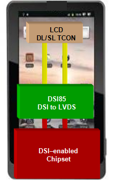
The SN65DSI85 DSI to FlatLink bridge features a dual-channel MIPI D-PHY receiver front-end configuration with 4 lanes per channel operating at 1 Gbps per lane; a maximum input bandwidth of 8 Gbps. The bridge decodes MIPI DSI 18-bpp RGB666 and 24-bpp RGB888 packets and converts the formatted video data stream to a FlatLink compatible LVDS output operating at pixel clocks operating from 25 MHz to 154 MHz, offering a Dual-Link LVDS, Single-Link LVDS, or two Single-Link LVDS interface(s) with four data lanes per link.
The SN65DSI85 is well suited for WQXGA (2560 × 1600) at 60 frames per second, as well as 3D Graphics at WUXGA and True HD (1920 × 1080) resolutions at an equivalent 120 fps with up to 24 bits-per-pixel. Partial line buffering is implemented to accommodate the data stream mismatch between the DSI and LVDS interfaces.
Designed with industry-compliant interface technology, the SN65DSI85 is compatible with a wide range of micro-processors, and is designed with a range of power management features including low-swing LVDS outputs, and the MIPI® defined ultra-low power state (ULPS) support.
The SN65DSI85 is implemented in a small outline 5-mm × 5-mm PBGA at 0.5-mm pitch package, and operates across a temperature range from –40ºC to 85ºC.
| PART NUMBER | PACKAGE | BODY SIZE (NOM) |
|---|---|---|
| SN65DSI85 | BGA MICROSTAR JUNIOR (64) | 5.00 mm × 5.00 mm |
- BQ24125 - 具有增强的 EMI 性能的单芯片开关模式、锂离子和锂聚合物充电管理 IC
- MSP430F248 - 16 位超低功耗微控制器,具有 48KB 闪存、4KB RAM、12 位 ADC、2 个 USCI 和 HW 乘法器
- LM5134 - 具有备用导频输出的单个 7.6A 峰值电流低侧栅极驱动器
- CD4504B-EP - 用于 TTL 到 CMOS 或 CMOS 到 CMOS 操作的 CMOS 六路电压电平转换器
- LP3944 - RGB/白光/蓝光 8 LED 趣味闪烁光驱动器
- SN74LV4040A - 12 位异步二进制计数器
- SN55183-SP - 抗辐射 V 类双路差动线路驱动器
- SN54LS90 - 十进制计数器
- DAC34SH84 - 四通道、16 位、1.5 GSPS 数模转换器 (DAC)。
- IVC102 - 精密交换式集成器互阻抗放大器

