



- UA78M05CKTPRG3 - 集成电路(IC) > 电源管理(PMIC) > 稳压器 - 线性
- LMV112SD-NS - 集成电路(IC) > 时钟/定时 > 时钟缓冲器,驱动器
- 84095012A - 集成电路(IC) > 逻辑 > 移位寄存器
- ADS7828E/250 - 集成电路(IC) > 数据采集 > 模数转换器(ADC)
- TUSB7320RKMR - 集成电路(IC) > 接口 > 控制器
- TLV320AIC3106IZQE - 集成电路(IC) > 接口 > 编解码器
- LP5900SDX-2.2 - 电源管理IC - 稳压器 - 线性
- TPS3780BDRYT - 集成电路(IC) > 电源管理(PMIC) > 监控器
- SN74LV373ADGSR - 集成电路(IC) > 逻辑 > 锁存器
- PCM1702PG4 - 集成电路(IC) > 数据采集 > ADC/DAC - 特殊用途
- LM3S6911-EQC50-A2 - 集成电路(IC) > 嵌入式 > 微控制器
- TLV2460CDRG4 - 集成电路(IC) > 线性 > 放大器 > 仪器,运算放大器,缓冲器
- TLV2464CNG4 - 集成电路(IC) > 线性 > 放大器 > 仪器,运算放大器,缓冲器
- LM3631YFFR - 集成电路(IC) > 电源管理(PMIC) > LED 驱动器
- ADC11C170HFEB/NOPB - 评估板 - 模数转换器(ADC)
- LMV7219M7/NOPB - 集成电路(IC) > 线性 > 比较器
- DAC8771RGZT - 集成电路(IC) > 数据采集 > 数模转换器(DAC)
- CLC404AJM5 - 集成电路(IC) > 线性 > 放大器 > 仪器,运算放大器,缓冲器
- PT7777C - 板安装电源 > 直流转换器
- 100122DCQR - 集成电路(IC) > 逻辑 > 缓冲器,驱动器,接收器,收发器



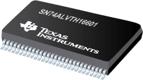
SN74ALVTH16601 - 具有三态输出的 2.5V/3.3V 18 位通用总线收发器
SN74ALVTH16601是TI德州仪器公司的一款通用总线收发器(UBT)产品,SN74ALVTH16601是具有三态输出的 2.5V/3.3V 18 位通用总线收发器,本站介绍了SN74ALVTH16601的封装应用图解、特点和优点、功能等,并给出了与SN74ALVTH16601相关的TI元器件型号供参考。
SN74ALVTH16601 - 具有三态输出的 2.5V/3.3V 18 位通用总线收发器 - 通用总线收发器(UBT) - 通用总线功能 - 德州仪器
The 'ALVTH16601 devices are 18-bit universal bus transceivers designed for 2.5-V or 3.3-V VCC operation, but with the capability to provide a TTL interface to a 5-V system environment.
The devices combine D-type latches and D-type flip-flops to allow data flow in transparent, latched, and clocked modes.
Data flow in each direction is controlled by output-enable (OEAB\ and OEBA\), latch-enable (LEAB and LEBA), and clock (CLKAB and CLKBA) inputs. The clock can be controlled by the clock-enable (CLKENAB\ and CLKENBA\) inputs. For A-to-B data flow, the device operates in the transparent mode when LEAB is high. When LEAB is low, the A data is latched if CLKAB is held at a high or low logic level. If LEAB is low, the A data is stored in the latch/flip-flop on the low-to-high transition of CLKAB. Output enable OEAB\ is active low. When OEAB\ is low, the outputs are active. When OEAB\ is high, the outputs are in the high-impedance state.
Data flow for B to A is similar to that of A to B, but uses OEBA\, LEBA, CLKBA, and CLKENBA\.
This device is fully specified for hot-insertion applications using Ioff and power-up 3-state. The Ioff circuitry disables the outputs, preventing damaging current backflow through the device when it is powered down. The power-up 3-state circuitry places the outputs in the high-impedance state during power up and power down, which prevents driver conflict.
When VCC is between 0 and 1.2 V, the device is in the high-impedance state during power up or power down. However, to ensure the high-impedance state above 1.2 V, OE\ should be tied to VCC through a pullup resistor; the minimum value of the resistor is determined by the current-sinking capability of the driver.
Active bus-hold circuitry is provided to hold unused or floating data inputs at a valid logic level.
The SN54ALVTH16601 is characterized for operation over the full military temperature range of -55°C to 125°C. The SN74ALVTH16601 is characterized for operation from -40°C to 85°C.
- UBTTM (Universal Bus Transceiver) Combines D-Type Latches and D-Type Flip-Flops for Operation in Transparent, Latched, Clocked, or Clock-Enabled Mode
- State-of-the-Art Advanced BiCMOS Technology (ABT) WidebusTM Design for 2.5-V and 3.3-V Operation and Low Static-Power Dissipation
- Support Mixed-Mode Signal Operation (5-V Input and Output Voltages With 2.3-V to 3.6-V VCC)
- Typical VOLP (Output Ground Bounce) <0.8 V at VCC = 3.3 V, TA = 25°C
- High-Drive (-24/24 mA at 2.5-V and -32/64 mA at 3.3-V VCC)
- Ioff and Power-Up 3-State Support Hot Insertion
- Use Bus Hold on Data Inputs in Place of External Pullup/Pulldown Resistors to Prevent the Bus From Floating
- Auto3-State Eliminates Bus Current Loading When Output Exceeds VCC + 0.5 V
- Flow-Through Architecture Facilitates Printed Circuit Board Layout
- Distributed VCC and GND Pin Configuration Minimizes High-Speed Switching Noise
- ESD Protection Exceeds 2000 V Per MIL-STD-883, Method 3015; Exceeds 200 V Using Machine Model (C = 200 pF, R = 0)
- Latch-Up Performance Exceeds 100 mA Per JESD 78, Class II
- Package Options Include Plastic Shrink Small-Outline (DL), Thin Shrink Small-Outline (DGG), Thin Very Small-Outline (DGV) Packages, and 380-mil Fine-Pitch Ceramic Flat (WD) Package
NOTE: For tape and reel order entry: The DGGR package is abbreviated to GR and the DGVR package is abbreviated to VR. UBT and Widebus are trademarks of Texas Instruments Incorporated.
- TLC1541 - 10 位 32kSPS ADC 串行输出微处理器外设/独立、11 通道
- TLV320AIC24K - 立体声低功耗语音频带编解码器
- TPS2022 - 1.1A 2.7-5.5V 单路配电开关 IC 高侧 MOSFET,具有故障报告和工作态低电平启用功能
- TPS77501-Q1 - 汽车类快速瞬态响应 500mA 低压降稳压器
- TPS92690-Q1 - 用于具有低侧电流感应功能的可调光 LED 驱动的汽车类 N 通道控制器
- TPS82693 - 700 mA、高效 MicroSiP 降压转换器(截面 <1mm)
- TS3USB221A - 具有单独使能和 ESD 保护的高速 USB 2.0 1:2 多路复用/多路解复用开关
- MSP430FR5888 - MSP430FR5888 混合信号微处理器
- CD4044B-MIL - 具有三态输出的 CMOS 四路与非 R/S 锁存器
- MSP430F47163 - 16 位超低功耗微处理器,具有 92KB 闪存、4KB RAM、3 个 Σ-Δ ADC 和 LCD 驱动器

