

- TMS320C6416TBCLZ7 - 集成电路(IC) > 嵌入式 > DSP(数字信号处理器)
- ADS6123IRHB25 - 集成电路(IC) > 数据采集 > 模数转换器(ADC)
- ISO7721FQDQ1 - 隔离器 > 数字隔离器
- REG711EA-2.7/2K5 - 集成电路(IC) > 电源管理(PMIC) > 稳压器 - DC-DC 开关稳压器
- TPS7A0331PDBVR - 电源管理IC - 稳压器 - 线性
- TMS320VC5502GZZ300 - 集成电路(IC) > 嵌入式 > DSP(数字信号处理器)
- MC33063ADG4 - 集成电路(IC) > 电源管理(PMIC) > 稳压器 - DC-DC 开关稳压器
- TPD4S214YFFR - 电路保护 > 浪涌抑制 IC
- LM2901PWG4 - 集成电路(IC) > 线性 > 比较器
- LM4040A50IDBZTG4 - 集成电路(IC) > 电源管理(PMIC) > 电压基准
- TMS320C6747CZKBA3 - 集成电路(IC) > 嵌入式 > DSP(数字信号处理器)
- TPA6040A4EVM - 开发板,套件,编程器 > 评估板 > 音频放大器评估板
- LM4674ATLX/NOPB - 集成电路(IC) > 线性 > 放大器 > 音频放大器
- LM64460BPPQRYFRQ1 - 集成电路(IC) > 电源管理(PMIC) > 稳压器 - DC-DC 开关稳压器
- PT4521A - 板安装电源 > 直流转换器
- ULN2003ANS - 分立半导体产品 > 晶体管 > 双极(BJT) > 双极晶体管阵列
- CC110LRTKT - 射频和无线 > 射频收发器 IC
- REG103FA-2.5 - 集成电路(IC) > 电源管理(PMIC) > 稳压器 - 线性
- REF3430QDBVRQ1 - 集成电路(IC) > 电源管理(PMIC) > 电压基准
- LMV611MF/NOPB - 集成电路(IC) > 线性 > 放大器 > 仪器,运算放大器,缓冲器
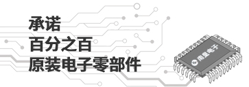


SN74AUP1T32 - 低功耗、1.8/2.5/3.3V 输入、3.3V CMOS 输出、2 输入正或门
SN74AUP1T32是TI德州仪器公司的一款无产品,SN74AUP1T32是低功耗、1.8/2.5/3.3V 输入、3.3V CMOS 输出、2 输入正或门,本站介绍了SN74AUP1T32的封装应用图解、特点和优点、功能等,并给出了与SN74AUP1T32相关的TI元器件型号供参考。
SN74AUP1T32 - 低功耗、1.8/2.5/3.3V 输入、3.3V CMOS 输出、2 输入正或门 - 无 - 小尺寸逻辑器件 - 德州仪器
- Single-Supply Voltage Translator
- Output Level Up to Supply VCC CMOS Level
- 1.8 V to 3.3 V (at VCC = 3.3 V)
- 2.5 V to 3.3 V (at VCC = 3.3 V)
- 1.8 V to 2.5 V (at VCC = 2.5 V)
- 3.3 V to 2.5 V (at VCC = 2.5 V
- Schmitt-Trigger Inputs Reject Input Noise and Provide Better Output Signal Integrity
- Ioff Supports Partial Power Down (VCC = 0 V)
- Very Low Static Power Consumption: 0.1 µA
- Very Low Dynamic Power Consumption: 0.9 µA
- Latch-Up Performance Exceeds 100 mA Per JESD 78, Class II
- Pb-Free Packages Available: SC-70 (DCK) 2 × 2.1 × 0.65 mm (Height 1.1 mm)
- More Gate Options Available at www.ti.com/littlelogic
- ESD Performance Tested Per JESD 22
- 2000-V Human-Body Model (A114-B, Class II)
- 1000-V Charged-Device Model (C101)
DESCRIPTION/ORDERING INFORMATION
The SN74AUP1T32 performs the Boolean function Y = A + B or Y = A\ • B\ with designation for logic-level translation applications with output referenced to supply VCC.
AUP technology is the industry’s lowest-power logic technology designed for use in extending battery-life in operating. All input levels that accept 1.8-V LVCMOS signals, while operating from either a single 3.3-V or 2.5-V VCC supply. This product also maintains excellent signal integrity (see Figure 1 and Figure 2).
The wide VCC range of 2.3 V to 3.6 V allows the possibility of switching output level to connect to external controllers or processors.
Schmitt-trigger inputs (VT = 210 mV between positive and negative input transitions) offer improved noise immunity during switching transitions, which is especially useful on analog mixed-mode designs. Schmitt-trigger inputs reject input noise, ensure integrity of output signals, and allow for slow input signal transition.
Ioff is a feature that allows for powered-down conditions (VCC = 0 V) and is important in portable and mobile applications. When VCC = 0 V, signals in the range from 0 V to 3.6 V can be applied to the inputs and outputs of the device. No damage occurs to the device under these conditions.
The SN74AUP1T32 is designed with optimized current-drive capability of 4 mA to reduce line reflections, overshoot, and undershoot caused by high-drive outputs.
- SN65LVDT390 - 四路 LVDS 接收器
- SN74AHC1G14 - 单路施密特触发反向器闸
- SN54ALS857 - 具有三态输出的六路 2 至 1 通用多路复用器
- SN54S175 - 具有清零功能的四路 D 类触发器
- CSD17327Q5A - 30V N 通道 NexFET? 功率 MOSFET
- LP2981A-33 - 具有关断状态的 100mA 超低压降稳压器,0.75% 容差]]
- UCC27423 - 具有启动的双路 4A MOSFET 驱动器
- SN65LVDS4 - 高速差动线路驱动器/接收器
- SN54ABT573 - 具有三态输出的八路透明 D 类锁存器
- TMS320C6424 - 定点数字信号处理器

