



- SN74AUP1G08DCKRE4 - 集成电路(IC) > 逻辑 > 门和反相器
- CC2620F128RSMR - 射频和无线 > 射频收发器 IC
- TLVH431CLP - 集成电路(IC) > 电源管理(PMIC) > 电压基准
- CLC432AJP - 集成电路(IC) > 线性 > 放大器 > 仪器,运算放大器,缓冲器
- RM48L940ZWTT - 集成电路(IC) > 嵌入式 > 微控制器
- LM25575QMH/NOPB - 集成电路(IC) > 电源管理(PMIC) > 稳压器 - DC-DC 开关稳压器
- PDRV8305NQPHPRQ1 - 集成电路(IC) > 电源管理(PMIC) > 栅极驱动器
- SN74HC109NE4 - 集成电路(IC) > 逻辑 > 触发器
- OPA363IDBVR - 集成电路(IC) > 线性 > 放大器 > 仪器,运算放大器,缓冲器
- UCC3803D - 集成电路(IC) > 电源管理(PMIC) > DC-DC 开关控制器
- LM4051AIM3-1.2/NOPB - 集成电路(IC) > 电源管理(PMIC) > 电压基准
- TLV2773IDGS - 集成电路(IC) > 线性 > 放大器 > 仪器,运算放大器,缓冲器
- LP2985AIM5-2.0/NOPB - 集成电路(IC) > 电源管理(PMIC) > 稳压器 - 线性
- SN74AS245DWRE4 - 逻辑 - 缓冲器,驱动器,接收器,收发器
- TS5A3159ADCKR - 集成电路(IC) > 接口 > 模拟开关,多路复用器,解复用器
- SN74AHCT541PWG4 - 集成电路(IC) > 逻辑 > 缓冲器,驱动器,接收器,收发器
- PTH08T250WAST - 板安装电源 > 直流转换器
- PT6523R - 直流转换器
- LM7908CT - 集成电路(IC) > 电源管理(PMIC) > 稳压器 - 线性
- TPS2062DR-1 - 集成电路(IC) > 电源管理(PMIC) > 配电开关,负载驱动器



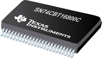
SN74CBT16800C - 具有预充电输出和 ?2V 下冲保护的 20 位 FET 总线开关
SN74CBT16800C是TI德州仪器公司的一款数字开关产品,SN74CBT16800C是具有预充电输出和 ?2V 下冲保护的 20 位 FET 总线开关,本站介绍了SN74CBT16800C的封装应用图解、特点和优点、功能等,并给出了与SN74CBT16800C相关的TI元器件型号供参考。
SN74CBT16800C - 具有预充电输出和 ?2V 下冲保护的 20 位 FET 总线开关 - 数字开关 - 信号开关 - 德州仪器
The SN74CBT16800C is a high-speed TTL-compatible FET bus switch with low ON-state resistance (ron), allowing for minimal propagation delay. Active Undershoot-Protection Circuitry on the A and B ports of the SN74CBT16800C provides protection for undershoot up to –2 V by sensing an undershoot event and ensuring that the switch remains in the proper OFF state. The device also precharges the B port to a user-selectable bias voltage (BIASV) to minimize live-insertion noise.
The SN74CBT16800C is organized as two 10-bit bus switches with separate output-enable (1OE\, 2OE\) inputs. It can be used as two 10-bit bus switches or as one 20-bit bus switch. When OE\ is low, the associated 10-bit bus switch is ON, and the A port is connected to the B port, allowing bidirectional data flow between ports. When OE\ is high, the associated 10-bit bus switch is OFF, and a high-impedance state exists between the A and B ports. The B port is precharged to BIASV through the equivalent of a 10-k resistor when OE\ is high, or if the device is powered down (VCC = 0 V).
During insertion (or removal) of a card into (or from) an active bus, the card’s output voltage may be close to GND. When the connector pins make contact, the card’s parasitic capacitance tries to force the bus signal to GND, creating a possible glitch on the active bus. This glitching effect can be reduced by using a bus switch with precharged bias voltage (BIASV) of the bus switch equal to the input threshold voltage level of the receivers on the active bus. This method will ensure that any glitch produced by insertion (or removal) of the card will not cross the input threshold region of the receivers on the active bus, minimizing the effects of live-insertion noise.
This device is fully specified for partial-power-down applications using Ioff. The Ioff feature ensures that damaging current will not backflow through the device when it is powered down.
To ensure the high-impedance state during power up or power down, OE\ should be tied to VCC through a pullup resistor; the minimum value of the resistor is determined by the current-sinking capability of the driver.
- Member of the Texas Instruments Widebus™ Family
- Undershoot Protection for Off-Isolation on A and B Ports Up To –2 V
- B-Port Outputs Are Precharged by Bias Voltage (BIASV) to Minimize Signal Distortion During Live Insertion and Hot-Plugging
- Supports PCI Hot Plug
- Bidirectional Data Flow, With Near-Zero Propagation Delay
- Low ON-State Resistance (ron) Characteristics (ron = 3 Typical)
- Low Input/Output Capacitance Minimizes Loading and Signal Distortion (Cio(OFF) = 5.5 pF Typical)
- Data and Control Inputs Provide Undershoot Clamp Diodes
- Low Power Consumption (ICC = 3 µA Max)
- VCC Operating Range From 4 V to 5.5 V
- Data I/Os Support 0 to 5-V Signaling Levels (0.8-V, 1.2-V, 1.5-V, 1.8-V, 2.5-V, 3.3-V, 5-V)
- Control Inputs Can Be Driven by TTL or 5-V/3.3-V CMOS Outputs
- Ioff Supports Partial-Power-Down Mode Operation
- Latch-Up Performance Exceeds 100 mA Per JESD 78, Class II
- ESD Performance Tested Per JESD 22
- 2000-V Human-Body Model (A114-B, Class II)
- 1000-V Charged-Device Model (C101)
- Supports Both Digital and Analog Applications: PCI Interface, Memory Interleaving, Bus Isolation, Low-Distortion Signal Gating
Widebus is a trademark of Texas Instruments.
- TPS7A6601-Q1 - 汽车类、高压、超低静态电流、低压降稳压器
- SN65LVDS179-EP - 高速差动线路驱动器和接收器
- ADS5277 - 8 通道 10 位 65MSPS 模数转换器
- MSP430F2013-EP - 增强型产品 16 位超低功耗微处理器,2kB 闪存、128B RAM、16 位 Σ-Δ A/D
- SN74LVTH182646A - 具有 18 位收发器和寄存器的 3.3V ABT 扫描测试设备
- LM2771 - 低纹波 250mA 开关电容器降压 DC/DC 转换器
- TPS3831G12 - 150nA 超低电流、超小型电压监控器
- ISO7242C - 四通道 2/2 25Mbps 数字隔离器
- LM8850 - 用于移动设备中高功率应用的高性能、升压 DC-DC 转换器
- ISO7221C-HT - 高温双通道 1/1 25Mbps 数字隔离器

