



- UC385TD-2 - 集成电路(IC) > 电源管理(PMIC) > 稳压器 - 线性
- SN74CB3Q3257DGVR - 集成电路(IC) > 逻辑 > 信号开关,多路复用器,解码器
- LM5160DNTJ - 集成电路(IC) > 电源管理(PMIC) > 稳压器 - DC-DC 开关稳压器
- ADS8598SIPM - 集成电路(IC) > 数据采集 > 模数转换器(ADC)
- TUSB4020BIPHPG4 - 集成电路(IC) > 接口 > 控制器
- TL5001AIDG4 - 集成电路(IC) > 电源管理(PMIC) > DC-DC 开关控制器
- THS6062IDRG4 - 集成电路(IC) > 接口 > 驱动器,接收器,收发器
- LP5522TM - 集成电路(IC) > 电源管理(PMIC) > LED 驱动器
- 76010012A - 集成电路(IC) > 逻辑 > 信号开关,多路复用器,解码器
- BQ2003STR - 集成电路(IC) > 电源管理(PMIC) > 电池充电器
- ADS127L21EVM-PDK - 开发板,套件,编程器 > 评估板 > 模数转换器(ADC)评估板
- TPS74617PQWDRBRQ1 - 集成电路(IC) > 电源管理(PMIC) > 稳压器 - 线性
- TLV61047EVM-038 - 开发板,套件,编程器 > 评估板 > DC/DC 和 AC/DC(离线)SMPS 评估板
- LM4562NA/NOPB - 集成电路(IC) > 线性 > 放大器 > 仪器,运算放大器,缓冲器
- TPS54428DRCR - 集成电路(IC) > 电源管理(PMIC) > 稳压器 - DC-DC 开关稳压器
- SCAN928028TUF/NOPB - 集成电路(IC) > 接口 > 串行器,解串器
- CD74AC323M - 集成电路(IC) > 逻辑 > 移位寄存器
- INA2143UA/2K5 - 集成电路(IC) > 线性 > 放大器 > 特殊用途放大器
- UA78L05AILPE3 - 集成电路(IC) > 电源管理(PMIC) > 稳压器 - 线性
- SN74ABT16500BDGGR - 集成电路(IC) > 逻辑 > 通用总线功能



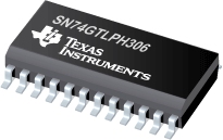
SN74GTLPH306 - 8 位 LVTTL 到 GTLP 总线收发器
SN74GTLPH306是TI德州仪器公司的一款无产品,SN74GTLPH306是8 位 LVTTL 到 GTLP 总线收发器,本站介绍了SN74GTLPH306的封装应用图解、特点和优点、功能等,并给出了与SN74GTLPH306相关的TI元器件型号供参考。
SN74GTLPH306 - 8 位 LVTTL 到 GTLP 总线收发器 - 无 - 背板逻辑器件(GTL/TTL/BTL/ECL收发器/转换器) - 德州仪器
The SN74GTLPH306 is a medium-drive, 8-bit bus transceiver that provides LVTTL-to-GTLP and GTLP-to-LVTTL signal-level translation. The device provides a high-speed interface between cards operating at LVTTL logic levels and a backplane operating at GTLP signal levels. High-speed (about three times faster than standard LVTTL or TTL) backplane operation is a direct result of GTLP's reduced output swing (<1 V), reduced input threshold levels, improved differential input, OEC™ circuitry, and TI-OPC™ circuitry. Improved GTLP OEC and TI-OPC circuits minimize bus-settling time and have been designed and tested using several backplane models. The medium drive allows incident-wave switching in heavily loaded backplanes with equivalent load impedance down to 19 .
GTLP is the Texas Instruments (TI™) derivative of the Gunning Transceiver Logic (GTL) JEDEC standard JESD 8-3. The ac specification of the SN74GTLPH306 is given only at the preferred higher-noise-margin GTLP, but the user has the flexibility of using this device at either GTL (VTT = 1.2 V and VREF = 0.8 V) or GTLP (VTT = 1.5 V and VREF = 1 V) signal levels.
Normally, the B port operates at GTLP signal levels. The A-port and control inputs operate at LVTTL logic levels, but are 5-V tolerant and are compatible with TTL and 5-V CMOS inputs. VREF is the B-port differential input reference voltage.
This device is fully specified for hot-insertion applications using Ioff and power-up 3-state. The Ioff circuitry disables the outputs, preventing damaging current backflow through the device when it is powered down. The power-up 3-state circuitry places the outputs in the high-impedance state during power up and power down, which prevents driver conflict.
This GTLP device features TI-OPC circuitry, which actively limits overshoot caused by improperly terminated backplanes, unevenly distributed cards, or empty slots during low-to-high signal transitions. This improves signal integrity, which allows adequate noise margin to be maintained at higher frequencies.
Active bus-hold circuitry holds unused or undriven LVTTL data inputs at a valid logic state. Use of pullup or pulldown resistors with the bus-hold circuitry is not recommended.
When VCC is between 0 and 1.5 V, the device is in the high-impedance state during power up or power down. However, to ensure the high-impedance state above 1.5 V, the output-enable (OE\) input should be tied to VCC through a pullup resistor; the minimum value of the resistor is determined by the current-sinking capability of the driver.
- TI-OPC™ Circuitry Limits Ringing on Unevenly Loaded Backplanes
- OEC™ Circuitry Improves Signal Integrity and Reduces Electromagnetic Interference
- Bidirectional Interface Between GTLP Signal Levels and LVTTL Logic Levels
- LVTTL Interfaces Are 5-V Tolerant
- Medium-Drive GTLP Outputs (50 mA)
- LVTTL Outputs (\x9624 mA/24 mA)
- GTLP Rise and Fall Times Designed for Optimal Data-Transfer Rate and Signal Integrity in Distributed Loads
- Ioff and Power-Up 3-State Support Hot Insertion
- Bus Hold on A-Port Data Inputs
- Latch-Up Performance Exceeds 100 mA Per JESD 78, Class II
- ESD Protection Exceeds JESD 22
- 2000-V Human-Body Model (A114-A)
- 200-V Machine Model (A115-A)
- 1000-V Charged-Device Model (C101)
OEC, TI, and TI-OPC are trademarks of Texas Instruments.
- TPS62090-Q1 - 汽车类:3A、2.5 至 6V 输入、效率高达 97%、3x3 QFN 降压转换器
- TPS22968 - 双通道、超低电阻负载开关,TPS22968
- MSP430F2616 - 16 位超低功耗 MCU,具有 92KB 闪存、4KB RAM、12 位 ADC、双 DAC、2 个 USCI、HW 乘法器和 DMA
- SN65HVD82 - 耐用的 RS-485 收发器
- BQ27425-G2B - 系统端 Impedance Track 电量监测计
- LM10507 - LM10507 三通道降压 + LDO 电源管理单元
- TPS24710 - 2.5V 至 18V 高效功率限制热插拔控制器
- UA78L09A - 3/8 引脚 100mA 固定 9V 正电压稳压器
- LM25574-Q1 - SIMPLE SWITCHER? 42V,0.5A 降压开关稳压器
- SN65LBC172A - 四路 RS-485 差动线路驱动器

