



- OPA549MKVC - 集成电路(IC) > 线性 > 放大器 > 仪器,运算放大器,缓冲器
- TPS629203EVM - 开发板,套件,编程器 > 评估板 > DC/DC 和 AC/DC(离线)SMPS 评估板
- TRSF3238CDWG4 - 接口 - 驱动器,接收器,收发器
- TPS22997EVM - 开发板,套件,编程器 > 评估板 > 评估和演示板及套件
- TLC59283RGET - 集成电路(IC) > 电源管理(PMIC) > LED 驱动器
- OPA548T-1 - 集成电路(IC) > 线性 > 放大器 > 仪器,运算放大器,缓冲器
- LM385BYZ-2.5/NOPB - 集成电路(IC) > 电源管理(PMIC) > 电压基准
- LM3674MFX-1.5 - 集成电路(IC) > 电源管理(PMIC) > 稳压器 - DC-DC 开关稳压器
- BQ501210RGCT - 集成电路(IC) > 电源管理(PMIC) > 电源管理 - 专用
- ADS7816PC - 集成电路(IC) > 数据采集 > 模数转换器(ADC)
- ISO7741FQDWWRQ1 - 隔离器 > 数字隔离器
- TLV2764CDR - 集成电路(IC) > 线性 > 放大器 > 仪器,运算放大器,缓冲器
- LM4990MH/NOPB - 集成电路(IC) > 线性 > 放大器 > 音频放大器
- 54F189DC - 集成电路(IC) > 存储器 > 存储器
- TPS22907YZTT - 集成电路(IC) > 电源管理(PMIC) > 配电开关,负载驱动器
- PT8139N - 直流转换器
- TLV320AIC24CPFBG4 - 集成电路(IC) > 接口 > 编解码器
- INA240A4D - 集成电路(IC) > 线性 > 放大器 > 仪器,运算放大器,缓冲器
- LMX1511TMX - 集成电路(IC) > 时钟/定时 > 时钟发生器,PLL,频率合成器
- 74FCT162H245CTPACT - 集成电路(IC) > 逻辑 > 缓冲器,驱动器,接收器,收发器



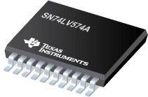
SN74LV574A - 具有三态输出的八路边沿 D 类触发器
SN74LV574A是TI德州仪器公司的一款D类触发器产品,SN74LV574A是具有三态输出的八路边沿 D 类触发器,本站介绍了SN74LV574A的封装应用图解、特点和优点、功能等,并给出了与SN74LV574A相关的TI元器件型号供参考。
SN74LV574A - 具有三态输出的八路边沿 D 类触发器 - D类触发器 - 触发器/锁存器/寄存器 - 德州仪器
The ’LV574A devices are octal edge-triggered D-type flip-flops designed for 2-V to 5.5-V VCC operation.
These devices feature 3-state outputs designed specifically for driving highly capacitive or relatively low-impedance loads. They are particularly suitable for implementing buffer registers, I/O ports, bidirectional bus drivers, and working registers.
On the positive transition of the clock (CLK) input, the Q outputs are set to the logic levels set up at the data (D) inputs.
A buffered output-enable (OE)\ input can be used to place the eight outputs in either a normal logic state (high or low logic levels) or high-impedance state. In the high-impedance state, the outputs neither load nor drive the bus lines significantly. The high-impedance state and the increased drive provide the capability to drive bus lines without need for interface or pullup components.
OE\ does not affect internal operations of the latch. Old data can be retained or new data can be entered while the outputs are in the high-impedance state.
To ensure the high-impedance state during power up or power down, OE\ should be tied to VCC through a pullup resistor; the minimum value of the resistor is determined by the current-sinking capability of the driver.
These devices are fully specified for partial-power-down applications using Ioff. The Ioff circuitry disables the outputs, preventing damaging current backflow through the devices when they are powered down.
- 2-V to 5.5-V VCC Operation
- Max tpd of 10 ns at 5 V
- Typical VOLP (Output Ground Bounce) <0.8 V at VCC = 3.3 V, TA = 25°C
- Typical VOHV (Output VOH Undershoot) >2.3 V at VCC = 3.3 V, TA = 25°C
- Supports Mixed-Mode Signal Operation on All Ports
- Ioff Supports Partial-Power-Down Mode Operation
- Latch-Up Performance Exceeds 250 mA Per JESD 17
- ESD Protection Exceeds JESD 22
- 2000-V Human-Body Model (A114-A)
- 200-V Machine Model (A115-A)
- 1000-V Charged-Device Model (C101)
- SN54LS373 - 具有三态输出的八路 D 类透明锁存器
- TPA6130A2 - 具有 I2C 音量控制的 138mW DirectPath 立体声耳机放大器 (TPA6130)
- TPS60242 - 具有固定 2.7V 输出用于 VCO 电源的 170 uVrms 零纹波开关电容升压转换器
- SN65HVD77 - 3.3V 电源 RS-485
- SN54LS195A - 4 位并行存取移位寄存器
- OPA376 - 低噪声、低 IQ 精密运算放大器
- TAS5715 - 具有扬声器均衡、双频带 DRC 和 DC 保护的 25W 立体声 I2S 音频放大器
- UC3524AM - 高级稳压脉宽调制器
- LM26480 - 外部可编程双路高电流降压 DC/DC 和双路线性稳压器
- TLC7705-Q1 - 汽车类微功耗电源电压监控器

