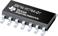

SN74LVC74A-Q1是TI公司的一款D类触发器产品,SN74LVC74A-Q1是汽车类具有清零和预设功能的双路上升沿 D 类触发器,本页介绍了SN74LVC74A-Q1的产品说明、应用、特性等,并给出了与SN74LVC74A-Q1相关的TI元器件型号供参考。
SN74LVC74A-Q1 - 汽车类具有清零和预设功能的双路上升沿 D 类触发器 - D类触发器 - 触发器/锁存器/寄存器 - TI公司(Texas Instruments,德州仪器)
- Qualified for Automotive Applications
- ESD Protection Exceeds 2000 V Per MIL-STD-883, Method 3015; Exceeds 200 V Using Machine Model (C = 200 pF, R = 0)
- Operates From 2 V to 3.6 V
- Inputs Accept Voltages to 5.5 V
- Max tpd of 5.2 ns at 3.3 V
- Typical VOLP (Output Ground Bounce) <0.8 V at VCC = 3.3 V, TA = 25°C
- Typical VOHV (Output VOH Undershoot)>2 V at VCC = 3.3 V, TA = 25°C
DESCRIPTION/ORDERING INFORMATION
The SN74LVC74A-Q1 dual positive-edge-triggered D-type flip-flop is designed for 2.7-V to 3.6-V VCC operation.
A low level at the preset (PRE) or clear (CLR) inputs sets or resets the outputs, regardless of the levels of the other inputs. When PRE and CLR are inactive (high), data at the data (D) input meeting the setup time requirements is transferred to the outputs on the positive-going edge of the clock pulse. Clock triggering occurs at a voltage level and is not directly related to the rise time of the clock pulse. Following the hold-time interval, data at the D input can be changed without affecting the levels at the outputs.
Inputs can be driven from either 3.3-V or 5-V devices. This feature allows the use of this device as a translator in a mixed 3.3-V/5-V system environment.


