



- LP3987ITLX-3.0 - 集成电路(IC) > 电源管理(PMIC) > 稳压器 - 线性
- DP83816-MAAP - 开发板,套件,编程器 > 评估板 > 评估和演示板及套件
- ESD451DPLR - 电路保护 > 瞬态电压抑制器(TVS) > TVS 二极管
- MLA00356DR - 集成电路(IC) > 线性 > 放大器 > 仪器,运算放大器,缓冲器
- CD40174BPWRE4 - 集成电路(IC) > 逻辑 > 触发器
- SN74ALVCH16500DLR - 集成电路(IC) > 逻辑 > 通用总线功能
- CD74HCT365M96 - 集成电路(IC) > 逻辑 > 缓冲器,驱动器,接收器,收发器
- LM3674MF-2.8 - 集成电路(IC) > 电源管理(PMIC) > 稳压器 - DC-DC 开关稳压器
- LM2598SX-5.0 - 集成电路(IC) > 电源管理(PMIC) > 稳压器 - DC-DC 开关稳压器
- ADC08134CIWMX - 集成电路(IC) > 数据采集 > 模数转换器(ADC)
- ADC10732CIWM - 集成电路(IC) > 数据采集 > 模数转换器(ADC)
- PTMA402050A1AS - 直流转换器
- LM3205SDX-2/NOPB - 集成电路(IC) > 电源管理(PMIC) > 稳压器 - DC-DC 开关稳压器
- UCC2804DR81221G4 - 集成电路(IC) > 电源管理(PMIC) > DC-DC 开关控制器
- LM2941T/LB08 - 集成电路(IC) > 电源管理(PMIC) > 稳压器 - 线性
- SN74LVC1G125DPWR - 集成电路(IC) > 逻辑 > 缓冲器,驱动器,接收器,收发器
- 74CBTLV16210VRE4 - 集成电路(IC) > 逻辑 > 信号开关,多路复用器,解码器
- SN74F241NSR - 集成电路(IC) > 逻辑 > 缓冲器,驱动器,接收器,收发器
- CDC6C020000ADLFRQ1 - 晶体,振荡器,谐振器 > 振荡器
- PT5812A - 直流转换器



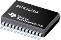
SN74LVC841A - 具有三态输出的 10 位总线接口 D 类锁存器
SN74LVC841A是TI德州仪器公司的一款D类锁存器产品,SN74LVC841A是具有三态输出的 10 位总线接口 D 类锁存器,本站介绍了SN74LVC841A的封装应用图解、特点和优点、功能等,并给出了与SN74LVC841A相关的TI元器件型号供参考。
SN74LVC841A - 具有三态输出的 10 位总线接口 D 类锁存器 - D类锁存器 - 触发器/锁存器/寄存器 - 德州仪器
This 10-bit bus-interface D-type latch is designed for 1.65-V to 3.6-V VCC operation.
The SN74LVC841A is designed specifically for driving highly capacitive or relatively low-impedance loads. It is particularly suitable for implementing buffer registers, I/O ports, bidirectional bus drivers, and working registers.
The ten latches are transparent D-type latches. The device has noninverting data (D) inputs and provides true data at its outputs.
A buffered output-enable (OE)\ input can be used to place the ten outputs in either a normal logic state (high or low logic levels) or a high-impedance state. In the high-impedance state, the outputs neither load nor drive the bus lines significantly. The high-impedance state and increased drive provide the capability to drive bus lines without interface or pullup components.
OE\ does not affect the internal operations of the latch. Previously stored data can be retained or new data can be entered while the outputs are in the high-impedance state.
Inputs can be driven from either 3.3-V or 5-V devices. This feature allows the use of these devices as translators in a mixed 3.3-V/5-V system environment.
To ensure the high-impedance state during power up or power down, OE\ should be tied to VCC through a pullup resistor; the minimum value of the resistor is determined by the current-sinking capability of the driver.
This device is fully specified for partial-power-down applications using Ioff. The Ioff circuitry disables the outputs, preventing damaging current backflow through the device when it is powered down.
- Operates From 1.65 V to 3.6 V
- Inputs Accept Voltages to 5.5 V
- Max tpd of 6.7 ns at 3.3 V
- Typical VOLP (Output Ground Bounce) <0.8 V at VCC = 3.3 V, TA = 25°C
- Typical VOHV (Output VOH Undershoot) >2 V at VCC = 3.3 V, TA = 25°C
- Ioff Supports Partial-Power-Down Mode Operation
- Supports Mixed-Mode Signal Operation on All Ports (5-V Input/Output Voltage With 3.3-V VCC)
- Latch-Up Performance Exceeds 250 mA Per JESD 17
- ESD Protection Exceeds JESD 22
- 2000-V Human-Body Model (A114-A)
- 200-V Machine Model (A115-A)
- 1000-V Charged-Device Model (C101)
- LM5134 - 具有备用导频输出的单个 7.6A 峰值电流低侧栅极驱动器
- TAS5711 - 具有扬声器均衡、DRC 和 2.1 支持的 20W 立体声 I2S 音频放大器
- ADS7883 - 2.7V-5.5V 12 位 3MSPS 串行 ADC
- DS90UB928Q-Q1 - 具有双向控制通道的 FPD-Link III 解串器
- SN74ABT8543 - 具有八路寄存总线收发器的扫描测试设备
- SN74BCT8374A - 具有八路 D 类边沿触发器的扫描测试设备
- LMK04110 - Clock Jitter Cleaner with Cascaded PLLs
- TPS7A1650-Q1 - 60V、5-μA IQ、100-mA 低压降稳压器
- SN74AVCBH324245 - 具有可配置电压转换和 3 态输出的 32 位双电源总线收发器
- TPS23785B - 具有绿色环保模式的高功耗、高效 PoE PD 和 DC-DC 控制器

