



- M0L1227QPMRQ1 - 集成电路(IC) > 嵌入式 > 微控制器
- SN74HCT138PWRE4 - 集成电路(IC) > 逻辑 > 信号开关,多路复用器,解码器
- TMS320F2806ZGMSR - 集成电路(IC) > 嵌入式 > 微控制器
- TPS76727QD - 集成电路(IC) > 电源管理(PMIC) > 稳压器 - 线性
- TWL6032A1B4YFFR - 集成电路(IC) > 电源管理(PMIC) > 电源管理 - 专用
- TLV5604IPW - 集成电路(IC) > 数据采集 > 数模转换器(DAC)
- XTR106UA/2K5 - 集成电路(IC) > 接口 > 传感器和检测器接口
- CDCEL949PERF-EVM - 开发板,套件,编程器 > 评估板 > 评估和演示板及套件
- TPS2819QDBVRQ1 - 集成电路(IC) > 电源管理(PMIC) > 栅极驱动器
- LM9061M/NOPB - 集成电路(IC) > 电源管理(PMIC) > 栅极驱动器
- MSP430FR2675TRHAT - 集成电路(IC) > 嵌入式 > 微控制器
- TMS320DM6441BZWT - 集成电路(IC) > 嵌入式 > DSP(数字信号处理器)
- TLV2763IDGS - 集成电路(IC) > 线性 > 放大器 > 仪器,运算放大器,缓冲器
- MSP430F6637IZQWR - 集成电路(IC) > 嵌入式 > 微控制器
- OPA861IDBVRG4 - 集成电路(IC) > 线性 > 放大器 > 仪器,运算放大器,缓冲器
- LP2989AIMM-3.3/NOPB - 集成电路(IC) > 电源管理(PMIC) > 稳压器 - 线性
- SN74HC163DRE4 - 集成电路(IC) > 逻辑 > 计数器,除法器
- OPA2320SAIDGSR - 集成电路(IC) > 线性 > 放大器 > 仪器,运算放大器,缓冲器
- JM38510/00502BCA - 集成电路(IC) > 逻辑 > 门和反相器
- TMS320DM6433ZDU5 - 嵌入式 - DSP(数字信号处理器)



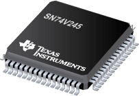
SN74V245 - 4096 x 18 同步 FIFO 存储器
SN74V245是TI德州仪器公司的一款FIFO寄存器产品,SN74V245是4096 x 18 同步 FIFO 存储器,本站介绍了SN74V245的封装应用图解、特点和优点、功能等,并给出了与SN74V245相关的TI元器件型号供参考。
SN74V245 - 4096 x 18 同步 FIFO 存储器 - FIFO寄存器 - 触发器/锁存器/寄存器 - 德州仪器
The SN74V215, SN74V225, SN74V235, and SN74V245 are very high-speed, low-power CMOS clocked first-in first-out (FIFO) memories. They support clock frequencies up to 133 MHz and have read-access times as fast as 5 ns. These DSP-Sync™ FIFO memories feature read and write controls for use in applications such as DSP-to-processor communication, DSP-to-analog front end (AFE) buffering, network, video, and data communications.
These are synchronous FIFOs, which means each port employs a synchronous interface. All data transfers through a port are gated to the low-to-high transition of a continuous (free-running) port clock by enable signals. The continuous clocks for each port are independent of one another and can be asynchronous or coincident. The enables for each port are arranged to provide a simple interface between DSPs, microprocessors, and/or buses controlled by a synchronous interface. An output-enable (OE)\ input controls the 3-state output.
The synchronous FIFOs have two fixed flags, empty flag/output ready (EF\/OR\) and full flag/input ready (FF\/IR\), and two programmable flags, almost-empty (PAE)\ and almost-full (PAF)\. The offset loading of the programmable flags is controlled by a simple state machine, and is initiated by asserting the load pin (LD)\. A half-full flag (HF)\ is available when the FIFO is used in a single-device configuration.
Two timing modes of operation are possible with these devices: first-word fall-through (FWFT) mode and standard mode.
In FWFT mode, the first word written to an empty FIFO is clocked directly to the data output lines after three transitions of the RCLK signal. A read enable (REN)\ does not have to be asserted for accessing the first word.
In standard mode, the first word written to an empty FIFO does not appear on the data output lines unless a specific read operation is performed. A read operation, which consists of activating REN\ and enabling a rising RCLK edge, shifts the word from internal memory to the data output lines.
These devices are depth expandable, using a daisy-chain technique or FWFT mode. The XI\ and XO\ pins are used to expand the FIFOs. In depth-expansion configuration, first load (FL)\ is grounded on the first device and set to high for all other devices in the daisy chain.
The SN74V215, SN74V225, SN74V235, and SN74V245 are characterized for operation from 0°C to 70°C.
- 512 × 18-Bit Organization Array (SN74V215)
- 1024 × 18-Bit Organization Array (SN74V225)
- 2048 × 18-Bit Organization Array (SN74V235)
- 4096 × 18-Bit Organization Array (SN74V245)
- 7.5-ns Read/Write Cycle Time
- 3.3-V VCC, 5-V Input Tolerant
- First-Word or Standard Fall-Through Timing
- Single or Double Register-Buffered Empty and Full Flags
- Easily Expandable in Depth and Width
- Asynchronous or Coincident Read and Write Clocks
- Asynchronous or Synchronous Programmable Almost-Empty and Almost-Full Flags With Default Settings
- Half-Full Flag Capability
- Output Enable Puts Output Data Bus in High-Impedance State
- High-Performance Submicron CMOS Technology
- Packaged in 64-Pin Thin Quad Flat Package
- DSP and Microprocessor Interface Control Logic
- Provide a DSP Glueless Interface to Texas Instruments TMS320™ DSPs
DSP-SYNC and TMS320 are trademarks of Texas Instruments.
- SN74LV02A - 四路 2 输入正与非门
- TMS320VC5441 - 数字信号处理器
- ADC104S021Q-Q1 - ADC104S021/21Q 4 通道、50 ksps 至 200 ksps、10 位 A/D 转换器
- TPS22986 - 电源选择 IC
- LM7815C - 15 Volt Regulator
- SN74HC151 - 8 线路到 1 线路数据选择器/多路复用器
- TPS54527 - 具有 D-CAP2 模式的 4.5V 至 18V 输入、5A 同步降压转换器
- SN54LS10 - 三路 3 输入正与非门
- SN74CBTLV16211 - 低电压 24 位 FET 总线开关
- DS90UB914A-Q1 - 25-100MHz 10/12 位 FPD-Link III 解串器

