



- SN74LS32DE4 - 集成电路(IC) > 逻辑 > 门和反相器
- LP3986TL-3133/NOPB - 电源管理IC - 稳压器 - 线性
- SN74BCT573NSRG4 - 集成电路(IC) > 逻辑 > 锁存器
- SN74V263-10GGM - 集成电路(IC) > 逻辑 > FIFO 存储器
- DEM-BUF-SO-1A - 开发板,套件,编程器 > 评估板 > 运算放大器评估板
- TLE2072QDRQ1 - 集成电路(IC) > 线性 > 放大器 > 仪器,运算放大器,缓冲器
- DS92LV1224TMSAX - 集成电路(IC) > 接口 > 串行器,解串器
- TPS2813PWR - 集成电路(IC) > 电源管理(PMIC) > 栅极驱动器
- LP8345IDT-1.8/NOPB - 集成电路(IC) > 电源管理(PMIC) > 稳压器 - 线性
- MCP810M3-4.38/NOPB - 电源管理IC - 监控器
- DRV11873EVM - 开发板,套件,编程器 > 评估板 > 评估和演示板及套件
- OPA2227UAG4 - 集成电路(IC) > 线性 > 放大器 > 仪器,运算放大器,缓冲器
- SN74LV4053ARGYR - 集成电路(IC) > 接口 > 模拟开关,多路复用器,解复用器
- BQ29414PWRG4 - 集成电路(IC) > 电源管理(PMIC) > 电池管理
- UCC28231PWR - 集成电路(IC) > 电源管理(PMIC) > DC-DC 开关控制器
- LM57EVM - 开发板,套件,编程器 > 评估板 > 传感器评估板
- SN74AHCT174DGVR - 逻辑 - 触发器
- TPS54620RHLR - 集成电路(IC) > 电源管理(PMIC) > 稳压器 - DC-DC 开关稳压器
- LT1013CPE4 - 集成电路(IC) > 线性 > 放大器 > 仪器,运算放大器,缓冲器
- CC1121RHMT - 射频和无线 > 射频收发器 IC


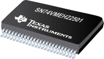
SN74VMEH22501 - 具有三态输出的 8 位通用总线收发器和两个 1 位总线收发器
SN74VMEH22501是TI德州仪器公司的一款通用总线收发器(UBT)产品,SN74VMEH22501是具有三态输出的 8 位通用总线收发器和两个 1 位总线收发器,本站介绍了SN74VMEH22501的封装应用图解、特点和优点、功能等,并给出了与SN74VMEH22501相关的TI元器件型号供参考。
SN74VMEH22501 - 具有三态输出的 8 位通用总线收发器和两个 1 位总线收发器 - 通用总线收发器(UBT) - 通用总线功能 - 德州仪器
- Member of the Texas Instruments Widebus™ Family
- UBT™ Transceiver Combines D-Type Latches and D-Type Flip-Flops for Operation in Transparent, Latched, or ClockedModes
- OEC™ Circuitry Improves Signal Integrity and Reduces Electromagnetic Interference (EMI)
- Compliant With VME64, 2eVME, and 2eSST Protocol
- Bus Transceiver Split LVTTL Port Provides a Feedback Path for Control and Diagnostics Monitoring
- I/O Interfaces Are 5-VTolerant
- B-Port Outputs (–48mA/64mA)
- Y and A-Port Outputs (–12mA/12mA)
- Ioff, Power-Up 3-State, and BIAS VCC Support LiveInsertion
- Bus Hold on 3A-Port Data Inputs
- 26- Equivalent Series Resistor on 3APorts and YOutputs
- Flow-Through Architecture Facilitates Printed Circuit Board Layout
- Distributed VCC and GND Pins Minimize High-Speed Switching Noise
- Latch-Up Performance Exceeds 100 mA Per JESD 78, ClassII
- ESD Protection Exceeds JESD 22
- 2000-V Human-Body Model (A114-A)
- 200-V Machine Model (A115-A)
- 1000-V Charged-Device Model (C101)
MicroStar is a trademark of Texas Instruments. (1) VME320 is a patented backplane construction by Arizona Digital, Inc.
DESCRIPTION/ORDERING INFORMATION
The SN74VMEH22501 8-bit universal bus transceiver has two integral 1-bit three-wire bus transceivers and is designed for 3.3-V VCC operation with 5-V tolerant inputs. The UBT™ transceiver allows transparent, latched, and flip-flop modes of data transfer, and the separate LVTTL input and outputs on the bus transceivers provide a feedback path for control and diagnostics monitoring. This device provides a high-speed interface between cards operating at LVTTL logic levels and VME64, VME64x, or VME320(1) backplane topologies.
High-speed backplane operation is a direct result of the improved OEC™ circuitry and high drive that has been designed and tested into the VME64x backplane model. The B-port I/Os are optimized for driving large capacitive loads and include pseudo-ETL input thresholds (½ VCC± 50 mV) for increased noise immunity. These specifications support the 2eVME protocols in VME64x (ANSI/VITA 1.1) and 2eSST protocols in VITA 1.5. With proper design of a 21-slot VME system, a designer can achieve 320-Mbyte transfer rates on linear backplanes and, possibly, 1-Gbyte transfer rates on the VME320 backplane.
All inputs and outputs are 5-V tolerant and are compatible with TTL and 5-V CMOS inputs.
Active bus-hold circuitry holds unused or undriven 3A-port inputs at a valid logic state. Bus-hold circuitry is not provided on 1A or 2A inputs, any B-port input, or any control input. Use of pullup or pulldown resistors with the bus-hold circuitry is not recommended.
This device is fully specified for live-insertion applications using Ioff, power-up 3-state, and BIAS VCC. The Ioff circuitry prevents damaging current to backflow through the device when it is powered off/on. The power-up 3-state circuitry places the outputs in the high-impedance state during power up and power down, which prevents driver conflict. The BIAS VCC circuitry precharges and preconditions the B-port input/output connections, preventing disturbance of active data on the backplane during card insertion or removal, and permits true live-insertion capability.
When VCC is between 0 and 1.5 V, the device is in the high-impedance state during power up or power down. However, to ensure the high-impedance state above 1.5 V, output-enable (OE and OEBY) inputs should be tied to VCC through a pullup resistor and output-enable (OEAB) inputs should be tied to GND through a pulldown resistor; the minimum value of the resistor is determined by the drive capability of the device connected to this input.
- SN74LS47 - BCD 到 7 段解码器/驱动器
- SN54HC165 - 并联负载 8 位移位寄存器
- CD54AC299 - 具有常见的并行 I/O 引脚和异步复位的 8 输入通用移位/存储寄存器
- TPS62130 - 采用 3x3 QFN 封装的具有 DCS 控制系统的 3-17V 3A 降压转换器
- LM8365 - 具有可编程输出延迟的微功耗欠压感应电路
- TPS3820-33-Q1 - 汽车类处理器监控电路
- SM320C6424-EP - 增强型产品定点数字信号处理器
- TPD2E001 - 用于高速数据接口的低电容 2 通道 +/-15KV ESD 保护阵列
- TL7759 - 用于 5V 系统的 4 终端 SVS
- TPS2202A - 具有串行接口的 1A 双槽 PC 卡电源开关

