



- TPS51116MPWPEP - 集成电路(IC) > 电源管理(PMIC) > 特殊用途稳压器
- SN74HCT273ANS - 集成电路(IC) > 逻辑 > 触发器
- TPS3851G25EQDRBRQ1 - 集成电路(IC) > 电源管理(PMIC) > 监控器
- TAS3202PAGR - 集成电路(IC) > 嵌入式 > DSP(数字信号处理器)
- TMP421AIDCNRG4 - 传感器,变送器 > 温度传感器 > 模拟和数字输出
- PCA9534ADW - 集成电路(IC) > 接口 > I/O 扩展器
- DAC80004IPWR - 集成电路(IC) > 数据采集 > 数模转换器(DAC)
- TMP102AIDRLT - 传感器,变送器 > 温度传感器 > 模拟和数字输出
- DRV5033FAQDBZR - 传感器,变送器 > 磁性传感器 > 开关(固态)
- LP3986TL-285285/NOPB - 集成电路(IC) > 电源管理(PMIC) > 稳压器 - 线性
- UCC5619MWPTR - 集成电路(IC) > 接口 > 信号端接器
- TPS65910A3A1RSLR - 集成电路(IC) > 电源管理(PMIC) > 电源管理 - 专用
- TL032AIDR - 集成电路(IC) > 线性 > 放大器 > 仪器,运算放大器,缓冲器
- TLV9022QDRQ1 - 集成电路(IC) > 线性 > 比较器
- TPS61121PWR - 电源管理IC - 电源管理 - 专用型
- TPS2051CDBVEVM-636 - 开发板,套件,编程器 > 评估板 > 评估和演示板及套件
- ADS5403EVM - 开发板,套件,编程器 > 评估板 > 模数转换器(ADC)评估板
- LM324J - 集成电路(IC) > 线性 > 放大器 > 仪器,运算放大器,缓冲器
- LT1014CNG4 - 集成电路(IC) > 线性 > 放大器 > 仪器,运算放大器,缓冲器
- SN74HC688DW - 集成电路(IC) > 逻辑 > 比较器



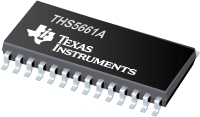
THS5661A - 12 位、125MSPS、CommsDAC、差动 介于 2mA 至 20mA 的可变电流输出
THS5661A是TI德州仪器公司的一款高速DAC(>10MSPS)产品,THS5661A是12 位、125MSPS、CommsDAC、差动 介于 2mA 至 20mA 的可变电流输出,本站介绍了THS5661A的封装应用图解、特点和优点、功能等,并给出了与THS5661A相关的TI元器件型号供参考。
THS5661A - 12 位、125MSPS、CommsDAC、差动 介于 2mA 至 20mA 的可变电流输出 - 高速DAC(>10MSPS) - 数模转换器 - 德州仪器
The THS5661A is a 12-bit resolution digital-to-analog converter (DAC) specifically optimized for digital data transmission in wired and wireless communication systems. The 12-bit DAC is a member of the CommsDAC series of high-speed, low-power CMOS digital-to-analog converters. The CommsDAC family consists of pin compatible 14-, 12-, 10-, and 8-bit DACs. All devices offer identical interface options, small outline package, and pinout. The THS5661A offers superior ac and dc performance while supporting update rates up to 125 MSPS.
The THS5661A operates from an analog and digital supply of 3 V to 5.5 V. Its inherent low power dissipation of 175 mW ensures that the device is well-suited for portable and low-power applications. Lowering the full-scale current output reduces the power dissipation without significantly degrading performance. The device features a SLEEP mode, which reduces the standby power to approximately 25 mW, thereby optimizing the power consumption for system needs.
The THS5661A is manufactured in Texas Instruments advanced high-speed mixed-signal CMOS process. A current-source-array architecture combined with simultaneous switching shows excellent dynamic performance. On-chip edge-triggered input latches and a 1.2 V temperature-compensated bandgap reference provide a complete monolithic DAC solution. The digital supply range of 3 V to 5.5 V supports 3 V and 5 V CMOS logic families. Minimum data input setup and hold times allow for easy interfacing with external logic. The THS5661A supports both a straight binary and twos complement input word format, enabling flexible interfacing with digital signal processors.
The THS5661A provides a nominal full-scale differential output current of 20 mA and < 300 k output impedance, supporting both single-ended and differential applications. The output current can be directly fed to the load (e.g., external resistor load or transformer), with no additional external output buffer required. An accurate on-chip reference and control amplifier allows the user to adjust this output current from 20 mA down to 2 mA, with no significant degradation of performance. This reduces power consumption and provides 20 dB gain range control capabilities. Alternatively, an external reference voltage and control amplifier may be applied in applications using a multiplying DAC. The output voltage compliance range is 1.25 V.
The THS5661A is available in both a 28-pin SOIC and TSSOP package. The device is characterized for operation over the industrial temperature range of –40°C to 85°C.
- Member of the Pin-Compatible CommsDAC™ Product Family
- 125 MSPS Update Rate
- 12-Bit Resolution
- Spurious Free Dynamic Range (SFDR) to Nyquist at 40 MHz Output: 60 dBc
- 1 ns Setup/Hold Time
- Differential Scalable Current Outputs: 2 mA to 20 mA
- On-Chip 1.2 V Reference
- 3 V and 5 V CMOS-Compatible Digital Interface
- Straight Binary or Twos Complement Input
- Power Dissipation: 175 mW at 5 V, Sleep Mode: 25 mW at 5 V
- Package: 28-Pin SOIC and TSSOP
CommsDAC is a trademark of Texas Instruments Incorporated.
- DCV010512D - 微型 1W 1500Vrms 隔离未稳压 DC/DC 转换器
- ADS54T02 - 12 位 800MSPS 2 通道反馈和接收器解决方案
- SN74HC251 - 具有三态输出的数据选择器/多路复用器
- LP2996A - LP2996 DDR 终端稳压器
- MSP430F67461A - MSP430F677x1A、MSP430F677x 1A、MSP430F677x1A 混合信号微控制器
- THS12082M - 12 位、8MSPS ADC,具有双通道、DSP/uP 接口、16X FIFO、通道自动扫描、低功耗
- DAC8831 - 16 位、超低功耗、电压输出数模转换器
- TPS61222-EP - 增强型产品,具有 5.5μA 静态电流的低输入电压、0.7V 升压转换器
- MSP430F2491 - 16 位超低功耗微控制器,具有 60KB 闪存、2KB RAM、2 个 USCI 和 HW 乘法器
- LM73605 - LM73605 SIMPLE SWITCHER? 3.5V 至 36V、5A 同步降压转换器

