



- PT4495C - 板安装电源 > 板安装电源配件
- ADS8910BRGET - 集成电路(IC) > 数据采集 > 模数转换器(ADC)
- LP8501TMX/NOPB - 集成电路(IC) > 电源管理(PMIC) > LED 驱动器
- TPS3703B5180DSERQ1 - 集成电路(IC) > 电源管理(PMIC) > 监控器
- SN74ALVCH373DGVR - 集成电路(IC) > 逻辑 > 锁存器
- TSB43AB21PDTG4 - 接口 - 控制器
- ADS7806U - 集成电路(IC) > 数据采集 > 模数转换器(ADC)
- TLC5947DAPR - 集成电路(IC) > 电源管理(PMIC) > LED 驱动器
- TPS2013PWRG4 - 集成电路(IC) > 电源管理(PMIC) > 配电开关,负载驱动器
- DAC8814EVM - 开发板,套件,编程器 > 评估板 > 数模转换器(DAC)评估板
- PCM1796DBR - 集成电路(IC) > 数据采集 > ADC/DAC - 特殊用途
- SN74LS540DBR - 集成电路(IC) > 逻辑 > 缓冲器,驱动器,接收器,收发器
- SN74LVC2952ANSRE4 - 逻辑 - 缓冲器,驱动器,接收器,收发器
- ADS7806P - 集成电路(IC) > 数据采集 > 模数转换器(ADC)
- TPS1101PWR - 分立半导体产品 > 晶体管 > FET,MOSFET > 单 FET,MOSFET
- LMV981IDCKRE4 - 集成电路(IC) > 线性 > 放大器 > 仪器,运算放大器,缓冲器
- CD74HCT123M96S5001 - 集成电路(IC) > 逻辑 > 多谐振荡器
- LMK6CE02500DDLER - 晶体,振荡器,谐振器 > 振荡器
- M0G3507QPMRQ1 - 集成电路(IC) > 嵌入式 > 微控制器
- LM10692BRMYT - 集成电路(IC) > 电源管理(PMIC) > 特殊用途稳压器



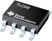
TLC548 - 8 位、45.5kSPS ADC,串行输出、低功耗、与 TLC540/545/1540 兼容、单通道
TLC548是TI德州仪器公司的一款精密ADC(<=10MSPS)产品,TLC548是8 位、45.5kSPS ADC,串行输出、低功耗、与 TLC540/545/1540 兼容、单通道,本站介绍了TLC548的封装应用图解、特点和优点、功能等,并给出了与TLC548相关的TI元器件型号供参考。
TLC548 - 8 位、45.5kSPS ADC,串行输出、低功耗、与 TLC540/545/1540 兼容、单通道 - 精密ADC(<=10MSPS) - 模数转换器 - 德州仪器
The TLC548 and TLC549 are CMOS analog-to-digital converter (ADC) integrated circuits built around an 8-bit switched-capacitor successive-approximation ADC. These devices are designed for serial interface with a microprocessor or peripheral through a 3-state data output and an analog input. The TLC548 and TLC549 use only the input/output clock (I/O CLOCK) input along with the chip select (CS\) input for data control. The maximum I/O CLOCK input frequency of the TLC548 is 2.048 MHz, and the I/O CLOCK input frequency of the TLC549 is specified up to 1.1 MHz.
Operation of the TLC548 and the TLC549 is very similar to that of the more complex TLC540 and TLC541 devices; however, the TLC548 and TLC549 provide an on-chip system clock that operates typically at 4 MHz and requires no external components. The on-chip system clock allows internal device operation to proceed independently of serial input/output data timing and permits manipulation of the TLC548 and TLC549 as desired for a wide range of software and hardware requirements. The I/O CLOCK together with the internal system clock allow high-speed data transfer and conversion rates of 45 500 conversions per second for the TLC548, and 40 000 conversions per second for the TLC549.
Additional TLC548 and TLC549 features include versatile control logic, an on-chip sample-and-hold circuit that can operate automatically or under microprocessor control, and a high-speed converter with differential high-impedance reference voltage inputs that ease ratiometric conversion, scaling, and circuit isolation from logic and supply noises. Design of the totally switched-capacitor successive-approximation converter circuit allows conversion with a maximum total error of ±0.5 least significant bit (LSB) in less than 17 us.
The TLC548C and TLC549C are characterized for operation from 0°C to 70°C. The TLC548I and TLC549I are characterized for operation from -40°C to 85°C.
- Microprocessor Peripheral or Standalone Operation
- 8-Bit Resolution A/D Converter
- Differential Reference Input Voltages
- Conversion Time . . . 17 us Max
- Total Access and Conversion Cycles Per Second - TLC548 . . . up to 45 500 - TLC549 . . . up to 40 000
- On-Chip Software-Controllable Sample-and-Hold Function
- Total Unadjusted Error . . . ±0.5 LSB Max
- 4-MHz Typical Internal System Clock
- Wide Supply Range . . . 3 V to 6 V
- Low Power Consumption . . . 15 mW Max
- Ideal for Cost-Effective, High-Performance Applications including Battery-Operated Portable Instrumentation
- Pinout and Control Signals Compatible With the TLC540 and TLC545 8-Bit A/D Converters and with the TLC1540 10-Bit A/D Converter
- CMOS Technology
- REF3140 - 采用 SOT23-3 封装最大漂移 20ppm/℃ 静态电流 100uA 的电压参考系列
- TPS3305-18 - 双路处理器监控电路
- TPS7A3001-EP - 增强型产品,-3V 至 -36V 输入电压、-200mA、超低噪声、高 PSRR、低压降线性稳压器
- LMP8645HV - Precision High Voltage Current Sense Amplifier
- SN74AS280 - 9 位奇偶校验发生器/校验器
- AM3715 - Sitara 处理器
- TPS2206A - 具有复位功能的 1A 双槽 PC 卡功率接口开关,用于串行 PCMCIA 控制器
- BQ24392-Q1 - 集成 USB2.0 开关、支持 BCDv1.2 的汽车充电器检测器件
- DAC7821 - 12 位并行输入乘法 DAC
- SN74LV11A - 三路 3 输入正与门

