



- SN65HVD1050DRG4 - 集成电路(IC) > 接口 > 驱动器,接收器,收发器
- TLV71315PDBVT - 集成电路(IC) > 电源管理(PMIC) > 稳压器 - 线性
- F280037CSPTG4 - 集成电路(IC) > 嵌入式 > 微控制器
- TPS53114PWP - 集成电路(IC) > 电源管理(PMIC) > DC-DC 开关控制器
- UC2879DW - 集成电路(IC) > 电源管理(PMIC) > AC DC 转换器,离线开关
- SN74CBT3244RGYR - 集成电路(IC) > 逻辑 > 信号开关,多路复用器,解码器
- SN74ABT2240ADW - 集成电路(IC) > 逻辑 > 缓冲器,驱动器,接收器,收发器
- LM2682MX/NOPB - 集成电路(IC) > 电源管理(PMIC) > 稳压器 - DC-DC 开关稳压器
- SN74ABT245BMDBREP - 集成电路(IC) > 逻辑 > 缓冲器,驱动器,接收器,收发器
- SN74LVC16244ADGGR - 集成电路(IC) > 逻辑 > 缓冲器,驱动器,接收器,收发器
- LM3S1162-EQC50-A2 - 集成电路(IC) > 嵌入式 > 微控制器
- AFE1230E/1KG4 - 数据采集 - 模拟前端(AFE)
- CDCU877ZQLT - 集成电路(IC) > 时钟/定时 > 应用特定时钟/定时
- DS90UA102TRHSJQ1 - 集成电路(IC) > 接口 > 串行器,解串器
- DAC7631EBG4 - 集成电路(IC) > 数据采集 > 数模转换器(DAC)
- LM4838LQX/NOPB - 集成电路(IC) > 线性 > 放大器 > 音频放大器
- DM74175N - 集成电路(IC) > 逻辑 > 触发器
- LDC1614QRGHTQ1 - 集成电路(IC) > 数据采集 > ADC/DAC - 特殊用途
- LM53635AQRNLRQ1 - 集成电路(IC) > 电源管理(PMIC) > 稳压器 - DC-DC 开关稳压器
- CC2430ZF128RTCRG3 - 射频和无线 > 射频收发器 IC



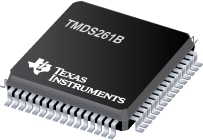
TMDS261B - 2 选 1 HDMI 开关
TMDS261B是TI德州仪器公司的一款DVI/HDMI产品,TMDS261B是2 选 1 HDMI 开关,本站介绍了TMDS261B的封装应用图解、特点和优点、功能等,并给出了与TMDS261B相关的TI元器件型号供参考。
TMDS261B - 2 选 1 HDMI 开关 - DVI/HDMI - 显示和成像串行器/解串器 - 德州仪器
The TMDS261B is a two-port digital video interface (DVI) or high-definition multimedia interface (HDMI) switch that allows up to two DVI or HDMI ports to be switched to a single display terminal. Four TMDS channels, one hot-plug detector, and a digital display control (DDC) interface are supported on each port. Each TMDS channel supports signaling rates up to 3 Gbps to allow 1080p resolution in 16-bit color depth. TMDS261B device is not intended for source side applications such as external switch boxes
The TMDS261B provides an adaptive equalizer for different ranges of cable lengths. The equalizer automatically compensates for intersymbol interference [ISI] loss of an HDMI/DVI cable for up to 20 dB at 3 Gbps (see ).
DLP is a trademark of Texas Instruments.
DescriptionWhen any of the input ports are selected, the integrated terminations (50-Ω termination resistors pulled up to VCC) are switched on for the TMDS clock channel, the TMDS clock-detection circuit is enabled, and the DDC repeater is enabled. After a valid TMDS clock is detected, the integrated termination resistors for the data lines are enabled, and the output TMDS lines are enabled. When an input port is not selected, the integrated terminations are switched off, the TMDS receivers are disabled, and the DDC repeater is disabled. Clock-detection circuitry provides an automatic power-management feature, because if no valid TMDS clock is detected, the terminations on the input TMDS data lines are disconnected and the TMDS outputs are placed in a high-impedance state.
The TMDS261B is designed to be controlled via a local I2C interface or GPIO interface, based on the status of the I2C_SEL pin. The local I2C interface in TMDS261B is a slave-only I2C interface. (See the section.)
I2C Mode: When the I2C_SEL pin is set low, the device is in I2C mode. With local I2C, the interface port status can be read, and the advanced configurations of the device such as TMDS output edge rate control, DDC I2C buffer output-voltage-select (OVS) settings (See the for detailed description on DDC I2C buffer description and OVS description), device power management, TMDS clock-detect feature, and TMDS input-port selection can be set..
GPIO mode: When the I2C_SEL pin is set high, the device is in GPIO control mode. The port selection is controlled with source selectors, S1 and S2. The power-saving mode is controlled through the LP pin. In GPIO mode, the default TMDS output edge rate that is the fastest setting of rise and fall time is set, and the default DDC I2C buffer OVS setting (OVS3) is set. See and the for a detailed description of the DDC I2C buffer.
Following are some of the key features (advantages) that the TMDS261B provides to the overall sink-side system (HDTV).
2×1 switch that supports TMDS data rates up to 3 Gbps on both input ports. ESD: Built-in support for high ESD protection (up to 10 kV on the HDMI source side). The HDMI source-side pins on the TMDS261B are connected via the HDMI/DVI exterior connectors and cable to the HDMI/DVI sources (e.g., DVD player). In TV applications, it can be expected that the source side may be subjected to higher ESD stresses compared to the sink side that is connected internally to the HDMI receiver. Adaptive equalization: The built-in adaptive equalization support compensates for intersymbol interference [ISI] loss of up to 20 dB, which represents a typical 20-m HDMI/DVI cable at 3 Gbps. Adaptive equalization adjusts the equalization gain automatically, based on the cable length and the incoming TMDS data rate. TMDS clock-detect circuitry: This feature provides an automatic power-management feature and also ensures that the TMDS output port is turned on only if there is a valid TMDS input signal. The TMDS clock-detect feature can be by-passed in I2C mode; see and . It is recommended to enable TMDS clock-detect circuitry during normal operation. However, for HDMI compliance testing (TMDS termination-voltage test), the clock-detect feature should be disabled by using the I2C mode control. If the customer requires passing the TMDS termination-voltage test in the GPIO mode with the default TMDS clock-detect circuitry enabled, then a valid TMDS clock should be provided for this compliance test, so that the terminations on the TMDS data pair can be connected and thus customer can pass the TMDS termination-voltage test. DDC I2C buffer: This feature provides isolation on the source-side and sink-side DDC I2C capacitance, thus helping the sink system to pass system-level compliance. Robust TMDS receive stage: This feature ensures that the TMDS261B can work with TMDS input signals having common-mode voltage levels that can be either compliant or non-compliant with HDMI/DVI specifications. VSadj: This feature adjusts the TMDS output swing and can help the sink system to tune the output TMDS swing of the TMDS261B (if needed) based on the system requirements. GPIO or local I2C interface to control the device features TMDS output edge-rate control: This feature adjusts the TMDS261B TMDS output rise and fall times. There are four settings of the rise and fall times that can be chosen. The default setting is the fastest rise and fall time; the other three settings are slower. Slower edge transitions can potentially help the sink system (HDTV) in passing regulatory EMI compliance.
- 2:1 Sink-side switch Supporting DVI Above 1920 × 1200 and HDMI HDTV Resolutions up to 1080p With 16-Bit Color Depth
- Designed for Signaling Rates up to 3 Gbps
- Supports HDMI 1.3a Specification
- Adaptive Equalization on inputs to support up to 20-m HDMI Cable at 2.25 Gbps for 1080p 12-Bit Color Depth
- TMDS Input Clock-Detect Circuit
- DDC Repeater Function
- <2-mW Low-Power Mode
- Local I2C or GPIO Configurable
- Enhanced ESD. HBM: 10 kV on All Input TMDS, DDC I2C, HPD Pins
- 3.3-Volt Power Supply
- Temperature Range: 0°C to 70°C
- 64-Pin TQFP Package: Pin-Compatible With TMDS251
- Robust TMDS Receive Stage That Can Work With Non-Compliant Input Common-Mode HDMI Signal
- APPLICATIONS
- High-Definition Digital TV
- LCD
- Plasma
- DLP
- High-Definition Digital TV
DLP is a trademark of Texas Instruments.
- CD74HCT4052 - 具有 TTL 输入的高速 CMOS 差动 4 通道模拟多路复用器/多路解复用器
- DAC122S085 - 具有轨至轨输出的 12 位微功耗双路数模转换器
- DRV104 - 用于螺线管、线圈、阀、加热器和电灯的 PWM 高侧驱动器 (1.5A)
- SN74SSTV32852-EP - 具有 Sstl_2 输入和输出的增强型产品 24 位至 48 位寄存缓冲器
- UCC38C43 - BiCMOS 低功耗电流模式 PWM 控制器
- LM4860 - 具有停机模式的 1 瓦音频功率放大器
- DAC7554 - 低功耗低短时脉冲波形干扰 12 位 DAC
- DLPC910 - 用于 DLP9000 和 DLP6500 DMD 的 DLPC910 数字控制器
- CD74HC423 - 具有复位功能的高速 CMOS 逻辑双路可重触发单稳多频振荡器
- SN65HVD267 - 含快速循环次数的 CAN 收发器,用于具有灵活数据速率的 CAN

